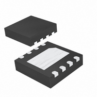
MAX4071ATA+T Maxim Integrated Products, MAX4071ATA+T Datasheet - Page 9

MAX4071ATA+T
Manufacturer Part Number
MAX4071ATA+T
Description
IC AMP CURRENT SENSE 8-TDFN
Manufacturer
Maxim Integrated Products
Datasheet
1.MAX4071ATAT.pdf
(18 pages)
Specifications of MAX4071ATA+T
Amplifier Type
Current Sense
Number Of Circuits
1
-3db Bandwidth
100kHz
Current - Input Bias
2.4µA
Voltage - Input Offset
80µV
Current - Supply
100µA
Voltage - Supply, Single/dual (±)
2.7 V ~ 24 V
Operating Temperature
-40°C ~ 125°C
Mounting Type
Surface Mount
Package / Case
8-TDFN Exposed Pad
Lead Free Status / RoHS Status
Lead free / RoHS Compliant
Output Type
-
Current - Output / Channel
-
Slew Rate
-
Gain Bandwidth Product
-
Other names
MAX4071ATA+T
MAX4071ATA+TTR
MAX4071ATA+TTR
MAX4069
10
—
1
2
3
4
5
6
7
8
9
MAX4070/
MAX4071
PIN
—
—
—
_______________________________________________________________________________________
1
2
3
4
5
6
7
8
Bidirectional, High-Side, Current-Sense
FROM BATTERY
MAX4072
LOAD
GAIN SELECT
CHARGER
SHUTDOWN
—
—
—
1
2
3
4
6
7
8
5
R
SENSE
REFOUT Reference Output Voltage (MAX4069/MAX4070/MAX4071)
NAME
REFIN
SHDN
GSEL
GND
OUT
RS+
N.C.
ADJ
V
RS-
CC
RS+
RS-
GSEL
SHDN
2.7V TO 24V
Shutdown Input. Drive SHDN low to select shutdown mode. Connect SHDN
to V
Negative Connection to the External Sense Resistor
Positive Connection to the External Sense Resistor
No Connection. Not internally connected.
Ground. For thin QFN packages, also make an external connection from
GND to the under-side exposed paddle.
Adjustable Output Voltage Feedback Input. Connect a resistor-divider
between REFOUT, ADJ, and GND (MAX4069 only, see Functional Diagram).
Voltage Output. The difference voltage, V
the voltage difference between RS+ and RS- and indicates the correct
polarity.
Supply Voltage Input. Bypass V
Gain-Setting Input. Connect GSEL low to select gain = 50V/V, or connect
GSEL high to select gain = 100V/V.
Reference Input Voltage (MAX4072)
V
CC
GND
CSA
CC
Amplifiers with Reference
for normal operation.
1.23V
V
REF
MAX4069
OA
REFOUT
OUT
ADJ
CC
FUNCTION
TO ADC
to GND with a 0.1µF capacitor.
R1
R2
OUT
Functional Diagram
- V
REF
Pin Description
, is proportional to
9


