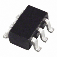
AD8027ARTZ-REEL7 Analog Devices Inc, AD8027ARTZ-REEL7 Datasheet - Page 19

AD8027ARTZ-REEL7
Manufacturer Part Number
AD8027ARTZ-REEL7
Description
IC OPAMP R-R LDIST LN LP SOT23-6
Manufacturer
Analog Devices Inc
Type
General Purpose Amplifierr
Datasheet
1.AD8027ARZ.pdf
(24 pages)
Specifications of AD8027ARTZ-REEL7
Slew Rate
100 V/µs
Amplifier Type
Voltage Feedback
Number Of Circuits
1
Output Type
Rail-to-Rail
-3db Bandwidth
190MHz
Current - Input Bias
4µA
Voltage - Input Offset
200µV
Current - Supply
6.5mA
Current - Output / Channel
120mA
Voltage - Supply, Single/dual (±)
2.7 V ~ 12 V, ±1.35 V ~ 6 V
Operating Temperature
-40°C ~ 125°C
Mounting Type
Surface Mount
Package / Case
SOT-23-6
Op Amp Type
High Speed
No. Of Amplifiers
1
Bandwidth
190MHz
Supply Voltage Range
2.7V To 12V
Amplifier Case Style
SOT-23
No. Of Pins
6
Rail/rail I/o Type
Rail to Rail Input/Output
Number Of Elements
1
Common Mode Rejection Ratio
90dB
Input Offset Voltage
900uV
Input Bias Current
6uA
Single Supply Voltage (typ)
3/5/9V
Dual Supply Voltage (typ)
±3/±5V
Voltage Gain In Db
105dB
Power Supply Rejection Ratio
90dB
Power Supply Requirement
Single/Dual
Shut Down Feature
Yes
Single Supply Voltage (min)
2.7V
Single Supply Voltage (max)
12V
Dual Supply Voltage (min)
±1.35V
Dual Supply Voltage (max)
±6V
Technology
Bipolar
Operating Temp Range
-40C to 125C
Operating Temperature Classification
Automotive
Mounting
Surface Mount
Pin Count
6
Package Type
SOT-23
Lead Free Status / RoHS Status
Lead free / RoHS Compliant
Gain Bandwidth Product
-
Lead Free Status / Rohs Status
Compliant
Other names
AD8027ARTZ-REEL7
Available stocks
Company
Part Number
Manufacturer
Quantity
Price
Company:
Part Number:
AD8027ARTZ-REEL7
Manufacturer:
AD
Quantity:
11 430
Part Number:
AD8027ARTZ-REEL7
Manufacturer:
ADI/亚德诺
Quantity:
20 000
WIDEBAND OPERATION
Voltage feedback amplifiers can use a wide range of resistor
values to set their gain. Proper design of the application’s
feedback network requires consideration of the following issues:
•
•
•
•
The AD8027/AD8028 have an input capacitance of 2 pF. This
input capacitance forms a pole with the amplifier’s feedback
network, destabilizing the loop. For this reason, it is generally
desirable to keep the source resistances below 500 Ω, unless
some capacitance is included in the feedback network. Likewise,
keeping the source resistances low also takes advantage of the
AD8027/AD8028’s low input referred voltage noise of
4.3 nV/√Hz.
With a wide bandwidth of over 190 MHz, the AD8027/AD8028
have numerous applications and configurations. The AD8027/
AD8028 part shown in Figure 57 is configured as a noninvert-
ing amplifier. An easy selection table of gain, resistor values,
bandwidth, slew rate, and noise performance is presented in
Table 5, and the inverting configuration is shown in Figure 58.
Table 5. Component Values, Bandwidth, and Noise
Performance (V
Noise Gain
(Noninverting)
1
2
10
Poles formed by the amplifier’s input capacitances with the
resistances seen at the amplifier’s input terminals
Effects of mismatched source impedances
Resistor value impact on the application’s voltage noise
Amplifier loading effects
Figure 57. Wideband Noninverting Gain Configuration
V
IN
R1 = R
R
S
G
= ±2.5 V)
R
(Ω)
50
50
50
SOURCE
R1
F
||R
G
–
+
AD8027/
AD8028
R
(Ω)
0
499
499
F
+V
–V
R
F
0.1μF
0.1μF
10μF
10μF
C1
C2
C3
C4
R
(Ω)
N/A
499
54.9
G
SELECT
–3 dB
SS BW
(MHz)
190
95
13
03327-A-056
V
OUT
Output
Noise with
Resistors
(nV/√Hz)
4.4
10
45
Rev. C | Page 19 of 24
CIRCUIT CONSIDERATIONS
Balanced Input Impedances
Balanced input impedances can help to improve distortion
performance. When the amplifier transitions from PNP pair to
NPN pair operation, a change in both the magnitude and
direction of the input bias current occurs. When multiplied
times imbalanced input impedances, a change in offset can
result. The key to minimizing this distortion is to keep the input
impedances balanced on both inputs. Figure 59 shows the effect
of the imbalance and degradation in distortion performance for
a 50 Ω source impedance, with and without a 50 Ω balanced
feedback path.
–100
–20
–30
–40
–50
–60
–70
–80
–90
R1 = R
0.1
V
Figure 58. Wideband Inverting Gain Configuration
G = +1
V
R
V
IN
OUT
S
L
R
C5
Figure 59. SFDR vs. Frequency and Various R
= 1kΩ
= +3V
F
F
= 0Ω
||R
= 2V p-p
R
G
G
R1
R
F
= 24.9Ω
–
AD8027/
+
AD8028
FREQUENCY (MHz)
1
+V
–V
R
R
C
F
F
F
= 49.9Ω
0.1μF
0.1μF
10μF
10μF
C1
C2
C3
C4
AD8027/AD8028
SELECT
03327-A-057
V
F
10
OUT
03327-A-058
20


