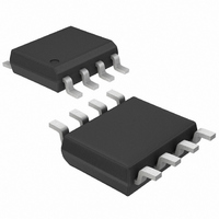
MAX4416ESA+ Maxim Integrated Products, MAX4416ESA+ Datasheet - Page 16

MAX4416ESA+
Manufacturer Part Number
MAX4416ESA+
Description
IC OPAMP DUAL +3/5V R-R 8-SOIC
Manufacturer
Maxim Integrated Products
Datasheet
1.MAX4415ESA.pdf
(22 pages)
Specifications of MAX4416ESA+
Amplifier Type
Voltage Feedback
Number Of Circuits
2
Output Type
Rail-to-Rail
Slew Rate
200 V/µs
-3db Bandwidth
400MHz
Current - Input Bias
1.3µA
Voltage - Input Offset
500µV
Current - Supply
1.6mA
Current - Output / Channel
75mA
Voltage - Supply, Single/dual (±)
2.7 V ~ 5.5 V
Operating Temperature
-40°C ~ 85°C
Mounting Type
Surface Mount
Package / Case
8-SOIC (3.9mm Width)
Number Of Channels
2
Voltage Gain Db
93 dB
Common Mode Rejection Ratio (min)
65 dB
Input Offset Voltage
0.5 mV
Operating Supply Voltage
3 V, 5 V
Maximum Power Dissipation
471 mW
Maximum Operating Temperature
+ 85 C
Mounting Style
SMD/SMT
Minimum Operating Temperature
- 40 C
Lead Free Status / RoHS Status
Lead free / RoHS Compliant
Gain Bandwidth Product
-
Lead Free Status / Rohs Status
Details
Coaxial cable and other transmission lines are easily
driven when properly terminated at both ends with their
characteristic impedance. Driving back-terminated
transmission lines essentially eliminates the line’s
capacitance.
___________Applications Information
The MAX4414/MAX4416/MAX4418 are internally com-
pensated for unity gain. When configured for unity gain,
the devices require a 24Ω feedback resistor (R
resistor improves AC response by reducing the Q of the
parallel LC circuit formed by the parasitic feedback
capacitance and inductance.
Low-Power, +3V/+5V, 400MHz Single-Supply
Op Amps with Rail-to-Rail Outputs
Figure 2. Capacitive Load vs. Isolation Resistance
16
Figure 1. Driving a Capacitive Load Through an Isolation
Resistor
______________________________________________________________________________________
30
28
26
24
22
20
18
16
14
12
10
R
V
G
IN
0
R
BIN
200
Choosing Resistor Values
400
C
LOAD
R
Unity-Gain Configuration
F
(pF)
600
800
R
ISO
1000
F
C
). This
V
L
OUT
Select the gain-setting feedback (R
resistor values that best fit the application. Large resis-
tor values increase voltage noise and interact with the
amplifier’s input and PC board capacitance. This can
generate undesirable poles and zeros and decrease
bandwidth or cause oscillations. For example, a nonin-
verting gain-of-two configuration (R
resistors, combined with 1.8pF of amplifier input capac-
itance and 1pF of PC board capacitance, causes a
pole at 114MHz. Since this pole is within the amplifier
bandwidth, it jeopardizes stability. Reducing the 1kΩ
resistors to 100Ω extends the pole frequency to
1.14GHz, but could limit output swing by adding 200Ω
in parallel with the amplifier’s load resistor.
Note: For high gain applications where output offset
voltage is a consideration, choose R
parallel combination of R
Figure 3a. Noninverting Gain Configuration
Figure 3b. Inverting Gain Configuration
IN
IN
Inverting and Noninverting Configurations
R
G
R
R
S
G
R
S
R
S
=
R
R
F
F
F
V
and R
OUT
×
+
R
F
V
= [1+ (R
OUT
R
R
R
F
G
G
= (R
G
F
F
(Figures 3a and 3b):
/ R
/ R
F
S
G
G
)] V
) V
F
= R
to be equal to the
) and input (R
IN
IN
G
V
) using 1kΩ
OUT
V
OUT
R
O
R
0
G
)


