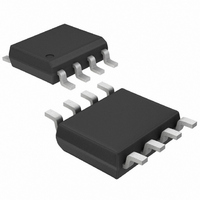
MAX4213ESA+ Maxim Integrated Products, MAX4213ESA+ Datasheet - Page 4

MAX4213ESA+
Manufacturer Part Number
MAX4213ESA+
Description
IC OP AMP R-R W/ENABLE 8-SOIC
Manufacturer
Maxim Integrated Products
Datasheet
1.MAX4213ESA.pdf
(16 pages)
Specifications of MAX4213ESA+
Amplifier Type
Voltage Feedback
Number Of Circuits
1
Output Type
Rail-to-Rail
Slew Rate
600 V/µs
-3db Bandwidth
300MHz
Current - Input Bias
5.4µA
Voltage - Input Offset
4000µV
Current - Supply
5.5mA
Current - Output / Channel
120mA
Voltage - Supply, Single/dual (±)
3.15 V ~ 11 V, ±1.575 V ~ 5.5 V
Operating Temperature
-40°C ~ 85°C
Mounting Type
Surface Mount
Package / Case
8-SOIC (3.9mm Width)
Number Of Channels
1
Common Mode Rejection Ratio (min)
70 dB
Input Offset Voltage
4 mV
Input Bias Current (max)
5.4 uA
Output Current (typ)
120 mA
Operating Supply Voltage
3.3 V, 5 V
Supply Current
5.5 mA
Maximum Power Dissipation
471 mW
Maximum Operating Temperature
+ 85 C
Minimum Operating Temperature
- 40 C
Dual Supply Voltage
+/- 3 V, +/- 5 V
Maximum Dual Supply Voltage
+/- 5.5 V
Minimum Dual Supply Voltage
+/- 1.575 V
Mounting Style
SMD/SMT
Shutdown
Yes
Supply Voltage (max)
11 V
Supply Voltage (min)
3.15 V
Voltage Gain Db
61 dB
Lead Free Status / RoHS Status
Lead free / RoHS Compliant
Gain Bandwidth Product
-
Lead Free Status / Rohs Status
Lead free / RoHS Compliant
Miniature, 300MHz, Single-Supply,
Rail-to-Rail Op Amps with Enable
AC ELECTRICAL CHARACTERISTICS
(V
noted.)
4
Note 1: Tested with V
Note 2: PSR for single 5V supply tested with V
Note 3: Does not include the external feedback network’s impedance.
Small-Signal -3dB Bandwidth
Large-Signal -3dB Bandwidth
Bandwidth for 0.1dB Gain
Flatness
Slew Rate
Settling Time to 0.1%
Rise/Fall Time
Spurious-Free Dynamic
Range
Harmonic Distortion
Two-Tone, Third-Order
Intermodulation Distortion
Input 1dB Compression Point
Differential Phase Error
Differential Gain Error
Input Noise-Voltage Density
Input Noise-Current Density
Input Capacitance
Disabled Output Capacitance
Output Impedance
Amplifier Enable Time
Amplifier Disable Time
Amplifier Gain Matching
Amplifier Crosstalk
CC
_______________________________________________________________________________________
= 5V, V
PARAMETER
V
CC
EE
= 4.5V to 5.5V; and for single 3.3V supply with V
= 0, V
CM
CM
= 2.5V, EN_ = 5V, R
= 2.5V.
C
SYMBOL
BW
OUT (OFF)
X
BW
BW
SFDR
Z
t
t
R
DG
C
t
HD
IP3
TALK
SR
DP
OFF
OUT
e
ON
t
0.1dB
i
, t
S
n
IN
n
SS
LS
F
F
= 24 , R
V
V
V
V
V
V
f
f
V
f1 = 10.0MHz, f2 = 10.1MHz, V
f
NTSC, R
NTSC, R
f = 10kHz
f = 10kHz
EN_ = 0
f = 10MHz
MAX4216/MAX4218/MAX4220,
f = 10MHz, V
MAX4216/MAX4218/MAX4220,
f = 10MHz, V
EE
C
C
C
OUT
OUT
OUT
OUT
OUT
OUT
OUT
= 5MHz, V
= 5MHz,
= 10MHz, A
= 0, V
= 20mV
= 2V
= 20mV
= 2V step
= 2V step
= 100mV
= 2V
L
L
CC
L
= 150
= 150
P-P
P-P
= 100
= 4.5V to 5.5V; for dual ±5V supply with V
OUT
OUT
OUT
P-P
P-P
VCL
P-P
EE
CONDITIONS
= 20mV
= 2V
= 2V
= 0, V
= 2
to V
P-P
P-P
CC
CC
MAX4212/MAX4213
MAX4216/MAX4218/
MAX4220
MAX4212/MAX4213
MAX4216/MAX4218/
MAX4220
2nd harmonic
3rd harmonic
Total harmonic
distortion
P-P
/2, V
= 3.15V to 3.45V.
OUT
OUT
= V
= 1V
CC
P-P
/2, A
VCL
= +1, T
MIN
EE
= -4.5V to -5.5V,
A
= +25°C, unless otherwise
TYP
0.02
0.02
300
200
180
600
100
-78
-78
-82
-75
1.3
0.1
-95
50
35
45
35
11
10
1
1
2
6
1
MAX
degrees
pA/ Hz
nV/ Hz
UNITS
dBm
MHz
MHz
MHz
V/µs
dBc
dBc
dBc
dB
dB
dB
ns
ns
pF
pF
ns
µs
%


