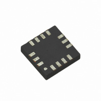
LMH6554LEE/NOPB National Semiconductor, LMH6554LEE/NOPB Datasheet - Page 14

LMH6554LEE/NOPB
Manufacturer Part Number
LMH6554LEE/NOPB
Description
IC OP AMP DIFF 2.8GHZ 14LLP
Manufacturer
National Semiconductor
Series
PowerWise®r
Datasheet
1.LMH6554LEENOPB.pdf
(16 pages)
Specifications of LMH6554LEE/NOPB
Amplifier Type
Differential
Number Of Circuits
1
Output Type
Differential
Slew Rate
6200 V/µs
-3db Bandwidth
2.8GHz
Current - Input Bias
1µA
Voltage - Input Offset
6500µV
Current - Supply
52mA
Current - Output / Channel
150mA
Voltage - Supply, Single/dual (±)
4.7 V ~ 5.25 V
Operating Temperature
-40°C ~ 125°C
Mounting Type
Surface Mount
Package / Case
14-LLP
No. Of Amplifiers
1
Input Offset Voltage
3mV
Bandwidth
2.8GHz
Supply Voltage Range
4.7V To 5.25V
Supply Current
52mA
Amplifier Case Style
LLP
No. Of Pins
14
Rohs Compliant
Yes
Lead Free Status / RoHS Status
Lead free / RoHS Compliant
Gain Bandwidth Product
-
Other names
LMH6554LEETR
www.national.com
Power Dissipation
The LMH6554 is optimized for maximum speed and perfor-
mance in a small form factor 14 lead LLP package. To ensure
maximum output drive and highest performance, thermal
shutdown is not provided. Therefore, it is of utmost impor-
tance to make sure that the T
the overall power dissipation.
Follow these steps to determine the maximum power dissi-
pation for the LMH6554:
1.
2.
3.
The maximum power that the LMH6554 package can dissi-
pate at a given temperature can be derived with the following
equation:
P
(°C) and θ
for a given package (°C/W). For the 14 lead LLP package,
θ
NOTE: If V
flowing in the feedback network. This current should be in-
JA
MAX
is 60°C/W.
FIGURE 9. Single Supply Bypassing Capacitors
Calculate the quiescent (no-load) power: P
(V
through the feedback network if V
Calculate the RMS power dissipated in each of the output
stages: P
((V
voltage and the current measured at the output pins of
the differential amplifier as if they were single ended
amplifiers and V
Calculate the total RMS power: P
= (150° − T
S
S
), where V
− V-
JA
CM
= Thermal resistance, from junction to ambient,
OUT
D
is not 0V then there will be quiescent current
(rms) = rms ((V
AMB
) * I-
S
= V
)/ θ
S
OUT
is the total supply voltage.
JA
+
− V
), where V
, where T
-
. (Be sure to include any current
JMAX
S
− V+
AMB
is never exceeded due to
OUT
OUT
= Ambient temperature
T
CM
and I
= P
) * I+
is not mid-rail).
AMP
OUT
30073264
OUT
+ P
AMP
are the
) + rms
D
= I
.
CC
*
14
cluded in the thermal calculations and added into the quies-
cent power dissipation of the amplifier.
ESD Protection
The LMH6554 is protected against electrostatic discharge
(ESD) on all pins. The LMH6554 will survive 2000V Human
Body model and 250V Machine model events. Under normal
operation the ESD diodes have no affect on circuit perfor-
mance. There are occasions, however, when the ESD diodes
will be evident. If the LMH6554 is driven by a large signal while
the device is powered down the ESD diodes will conduct . The
current that flows through the ESD diodes will either exit the
chip through the supply pins or will flow through the device,
hence it is possible to power up a chip with a large signal
applied to the input pins. Using the shutdown mode is one
way to conserve power and still prevent unexpected opera-
tion.
Board Layout
The LMH6554 is a high speed, high performance amplifier. In
order to get maximum benefit from the differential circuit ar-
chitecture board layout and component selection is very crit-
ical. The circuit board should have a low inductance ground
plane and well bypassed broad supply lines. External com-
ponents should be leadless surface mount types. The feed-
back network and output matching resistors should be
composed of short traces and precision resistors (0.1%). The
output matching resistors should be placed within 3 or 4 mm
of the amplifier as should the supply bypass capacitors. Refer
to the section titled Power Supply Bypassing for recommen-
dations on bypass circuit layout. Evaluation boards are avail-
able through the product folder on National’s web site.
By design, the LMH6554 is relatively insensitive to parasitic
capacitance at its inputs. Nonetheless, ground and power
plane metal should be removed from beneath the amplifier
and from beneath R
frequency.
With any differential signal path, symmetry is very important.
Even small amounts of asymmetry can contribute to distortion
and balance errors.
Evaluation Board
See the LMH6554 Product Folder on www.national.com for
evaluation board availability and ordering information.
F
and R
G
for best performance at high


