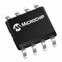
MCP6G03-E/MS Microchip Technology, MCP6G03-E/MS Datasheet - Page 9

MCP6G03-E/MS
Manufacturer Part Number
MCP6G03-E/MS
Description
IC GAIN BLOCK 1.8V 1CH 8MSOP
Manufacturer
Microchip Technology
Datasheet
1.MCP6G01UT-EOT.pdf
(38 pages)
Specifications of MCP6G03-E/MS
Amplifier Type
General Purpose
Number Of Circuits
1
Output Type
Rail-to-Rail
Slew Rate
4.5 V/µs
-3db Bandwidth
900kHz
Current - Input Bias
1pA
Voltage - Input Offset
1000µV
Current - Supply
110µA
Current - Output / Channel
20mA
Voltage - Supply, Single/dual (±)
1.8 V ~ 5.5 V
Operating Temperature
-40°C ~ 125°C
Mounting Type
Surface Mount
Package / Case
8-MSOP, Micro8™, 8-uMAX, 8-uSOP,
No. Of Amplifiers
1
Bandwidth
900kHz
No. Of Channels
1
Supply Voltage Range
1.8V To 5.5V
Amplifier Case Style
MSOP
No. Of Pins
8
Operating Temperature Range
-40°C To +125°C
Rohs Compliant
Yes
Lead Free Status / RoHS Status
Lead free / RoHS Compliant
Gain Bandwidth Product
-
Available stocks
Company
Part Number
Manufacturer
Quantity
Price
Company:
Part Number:
MCP6G03-E/MS
Manufacturer:
MICROCHIP
Quantity:
12 000
2.0
Note: Unless otherwise indicated, T
R
FIGURE 2-1:
FIGURE 2-2:
FIGURE 2-3:
© 2006 Microchip Technology Inc.
L
Note:
= 100 kΩ to V
20%
18%
16%
14%
12%
10%
14%
12%
10%
30%
25%
20%
15%
10%
8%
6%
4%
2%
0%
8%
6%
4%
2%
0%
5%
0%
TYPICAL PERFORMANCE CURVES
2460 Samples
G = +50
G = +10
G = +1
4916 Samples
G ≥ +10
2460 Samples
G = +1
The graphs and tables provided following this note are a statistical summary based on a limited number of
samples and are provided for informational purposes only. The performance characteristics listed herein
are not tested or guaranteed. In some graphs or tables, the data presented may be outside the specified
operating range (e.g., outside specified power supply range) and therefore outside the warranted range.
DD
/2, C
Input Offset Voltage (mV)
DC Gain Error, G = +1.
DC Gain Error, G ≥ +10.
Input Offset Voltage.
DC Gain Error (%)
DC Gain Error (%)
L
= 60 pF, GSEL = V
A
= +25°C, V
DD
/2, and CS is tied low.
DD
= +1.8V to +5.5V, V
MCP6G01/1R/1U/2/3/4
FIGURE 2-4:
FIGURE 2-5:
FIGURE 2-6:
14%
12%
10%
22%
20%
18%
16%
14%
12%
10%
18%
16%
14%
12%
10%
8%
6%
4%
2%
0%
8%
6%
4%
2%
0%
8%
6%
4%
2%
0%
1612 Samples
G = +1, +10, +50
T
2459 Samples
G = +1
T
A
A
= -40 to +125°C
SS
= -40 to +125°C
= GND, G = +1 V/V, V
Input Offset Voltage Drift (µV/°C)
DC Gain Drift (ppm/°C)
DC Gain Drift (ppm/°C)
DC Gain Drift, G = +1.
DC Gain Drift, G ≥ +10.
Input Offset Voltage Drift.
4912 Samples
G ≥ +10
T
A
= -40 to +125°C
DS22004B-page 9
IN
= (0.3V)/G,


