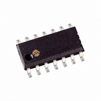
MCP6274-E/SL Microchip Technology, MCP6274-E/SL Datasheet - Page 5

MCP6274-E/SL
Manufacturer Part Number
MCP6274-E/SL
Description
IC OPAMP 2.0V QUAD R-R 14SOIC
Manufacturer
Microchip Technology
Specifications of MCP6274-E/SL
Slew Rate
0.9 V/µs
Package / Case
14-SOIC (3.9mm Width), 14-SOL
Amplifier Type
General Purpose
Number Of Circuits
4
Output Type
Rail-to-Rail
Gain Bandwidth Product
2MHz
Current - Input Bias
1pA
Voltage - Input Offset
3000µV
Current - Supply
170µA
Current - Output / Channel
25mA
Voltage - Supply, Single/dual (±)
2 V ~ 6 V
Operating Temperature
-40°C ~ 125°C
Mounting Type
Surface Mount
Number Of Channels
4
Common Mode Rejection Ratio (min)
70 dB
Input Offset Voltage
3 mV
Input Bias Current (max)
1 pA
Operating Supply Voltage
3 V, 5 V
Maximum Operating Temperature
+ 125 C
Minimum Operating Temperature
- 40 C
Mounting Style
SMD/SMT
Shutdown
No
Supply Voltage (max)
5.5 V
Supply Voltage (min)
2 V
Technology
CMOS
Voltage Gain Db
110 dB
Lead Free Status / RoHS Status
Lead free / RoHS Compliant
-3db Bandwidth
-
Lead Free Status / Rohs Status
Lead free / RoHS Compliant
Available stocks
Company
Part Number
Manufacturer
Quantity
Price
Company:
Part Number:
MCP6274-E/SL
Manufacturer:
MURATA
Quantity:
1 200
Part Number:
MCP6274-E/SL
Manufacturer:
MICROCHIP/微芯
Quantity:
20 000
Part Number:
MCP6274-E/SL/SOL342108
Manufacturer:
MICROCHIP/微芯
Quantity:
20 000
2.0
Note: Unless otherwise indicated, T
R
FIGURE 2-1:
FIGURE 2-2:
T
FIGURE 2-3:
Common Mode Input Voltage at V
2004 Microchip Technology Inc.
A
L
Note:
= 10 k
= +85°C.
-100
20%
18%
16%
14%
12%
10%
300
250
200
150
100
-50
8%
6%
4%
2%
0%
50
32%
28%
24%
20%
16%
12%
0
8%
4%
0%
TYPICAL PERFORMANCE CURVES
V
832 Samples
V
DD
422 Samples
T
0
The graphs and tables provided following this note are a statistical summary based on a limited number of
samples and are provided for informational purposes only. The performance characteristics listed herein
are not tested or guaranteed. In some graphs or tables, the data presented may be outside the specified
operating range (e.g., outside specified power supply range) and therefore outside the warranted range.
to V
CM
A
= 2.0V
= +85°C
= V
10
DD
SS
Common Mode Input Voltage (V)
/2 and C
20
Input Offset Voltage (mV)
Input Bias Current (pA)
Input Offset Voltage.
30
Input Bias Current at
Input Offset Voltage vs.
40
L
= 60 pF.
50
60
A
= +25°C, V
70
DD
T
T
T
T
A
A
A
A
= +125°C
= +85°C
= +25°C
=
= 2.0V.
80
-40°C
90
DD
100
= +2.0V to +5.5V, V
FIGURE 2-4:
FIGURE 2-5:
T
FIGURE 2-6:
Common Mode Input Voltage at V
A
= +125°C.
-100
14%
12%
10%
300
250
200
150
100
24%
20%
16%
12%
-50
8%
6%
4%
2%
0%
50
8%
4%
0%
0
SS
V
422 Samples
T
832 Samples
V
T
= GND, V
DD
MCP6271/2/3/4/5
A
CM
A
= +125°C
= -40°C to +125°C
= 5.5V
= V
SS
Common Mode Input Voltage (V)
Input Offset Voltage Drift (µV/°C)
CM
Input Bias Current (nA)
Input Offset Voltage Drift.
Input Bias Current at
Input Offset Voltage vs.
= V
DD
T
T
T
T
A
A
A
A
= +125°C
= +85°C
= +25°C
=
/2, V
-40°C
OUT
DS21810D-page 5
DD
= 5.5V.
V
DD
/2,


