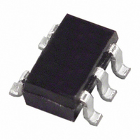
ADA4505-1ARJZ-R2 Analog Devices Inc, ADA4505-1ARJZ-R2 Datasheet - Page 6

ADA4505-1ARJZ-R2
Manufacturer Part Number
ADA4505-1ARJZ-R2
Description
IC OPAMP GP RRIO 50KHZ SOT23-5
Manufacturer
Analog Devices Inc
Datasheet
1.ADA4505-1ARJZ-R2.pdf
(24 pages)
Specifications of ADA4505-1ARJZ-R2
Slew Rate
0.006 V/µs
Amplifier Type
Voltage Feedback
Number Of Circuits
1
Output Type
Rail-to-Rail
Gain Bandwidth Product
50kHz
Current - Input Bias
0.5pA
Voltage - Input Offset
500µV
Current - Supply
9µA
Current - Output / Channel
40mA
Voltage - Supply, Single/dual (±)
1.8 V ~ 5 V, ±0.9 V ~ 2.5 V
Operating Temperature
-40°C ~ 125°C
Mounting Type
Surface Mount
Package / Case
SOT-23-5, SC-74A, SOT-25
Op Amp Type
Low Power
No. Of Amplifiers
1
Bandwidth
50kHz
Supply Voltage Range
± 0.9V To ± 2.5V
Amplifier Case Style
SOT-23
No. Of Pins
5
Lead Free Status / RoHS Status
Lead free / RoHS Compliant
-3db Bandwidth
-
Lead Free Status / RoHS Status
Lead free / RoHS Compliant, Lead free / RoHS Compliant
Other names
ADA4505-1ARJZ-R2TR
Available stocks
Company
Part Number
Manufacturer
Quantity
Price
Part Number:
ADA4505-1ARJZ-R2
Manufacturer:
ADI/亚德诺
Quantity:
20 000
ADA4505-1/ADA4505-2/ADA4505-4
TYPICAL PERFORMANCE CHARACTERISTICS
T
–1000
–1500
A
1500
1000
–500
= 25°C, unless otherwise noted.
500
0
0
140
120
100
14
12
10
V
80
60
40
20
8
6
4
2
0
Figure 9. Input Offset Voltage vs. Common-Mode Voltage
0
SY
–3.0 –2.5 –2.0 –1.5 –1.0 –0.5
0
0.2
= 1.8V
V
V
SY
CM
0.5 1.0
Figure 8. Input Offset Voltage Drift Distribution
= 1.8V
= V
Figure 7. Input Offset Voltage Distribution
0.4
SY
/2
1.5 2.0
0.6
0.8
V
CM
TCV
2.5 3.0 3.5
V
(V)
OS
1.0
OS
0
(µV/°C)
(mV)
0.5
1.2
4.0 4.5 5.0
1.0 1.5 2.0
1.4
V
–40°C ≤ T
SY
= 1.8V
1.6
A
≤ 125°C
5.5 6.0
2.5 3.0
1.8
DEVICE 1
DEVICE 2
DEVICE 3
DEVICE 4
DEVICE 5
DEVICE 6
DEVICE 7
DEVICE 8
DEVICE 9
DEVICE 10
Rev. D | Page 6 of 24
–1000
–1500
1500
1000
–500
500
0
0
140
120
100
V
14
12
10
80
60
40
20
Figure 12. Input Offset Voltage vs. Common-Mode Voltage
SY
8
6
4
2
0
0
–3.0 –2.5 –2.0 –1.5 –1.0 –0.5
0
= 5V
V
V
SY
CM
Figure 11. Input Offset Voltage Drift Distribution
0.5 1.0
= 5V
Figure 10. Input Offset Voltage Distribution
= V
1
SY
/2
1.5
2.0 2.5
2
V
CM
TCV
V
(V)
OS
OS
3.0 3.5
0
(µV/°C)
(mV)
3
0.5
4.0 4.5 5.0
1.0 1.5
V
–40°C ≤ T
SY
4
= 5V
2.0
A
≤ 125°C
5.5 6.0
2.5 3.0
5
DEVICE 1
DEVICE 2
DEVICE 3
DEVICE 4
DEVICE 5
DEVICE 6
DEVICE 7
DEVICE 8
DEVICE 9
DEVICE 10


