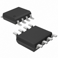
MAX4201ESA+ Maxim Integrated Products, MAX4201ESA+ Datasheet - Page 9

MAX4201ESA+
Manufacturer Part Number
MAX4201ESA+
Description
IC BUFFER OPEN LOOP 8-SOIC
Manufacturer
Maxim Integrated Products
Datasheet
1.MAX4200ESA.pdf
(14 pages)
Specifications of MAX4201ESA+
Amplifier Type
Buffer
Number Of Circuits
1
Slew Rate
4200 V/µs
-3db Bandwidth
780MHz
Current - Input Bias
800nA
Voltage - Input Offset
1000µV
Current - Supply
2.2mA
Current - Output / Channel
52mA
Voltage - Supply, Single/dual (±)
±4 V ~ 5.5 V
Operating Temperature
-40°C ~ 85°C
Mounting Type
Surface Mount
Package / Case
8-SOIC (3.9mm Width)
Number Of Channels
1
Input Offset Voltage
1 mV
Input Bias Current (max)
800 nA
Maximum Power Dissipation
471 mW
Maximum Operating Temperature
+ 85 C
Minimum Operating Temperature
- 40 C
Dual Supply Voltage
+/- 5 V
Maximum Dual Supply Voltage
+/- 5.5 V
Minimum Dual Supply Voltage
+/- 4 V
Mounting Style
SMD/SMT
Shutdown
No
Voltage Gain Db
6.02 dB
No. Of Amplifiers
1
Gain Bandwidth
780MHz
Supply Voltage Range
± 4V To ± 5.5V
Output Current
52mA
Amplifier Output
Single Ended
Rohs Compliant
Yes
Lead Free Status / RoHS Status
Lead free / RoHS Compliant
Output Type
-
Gain Bandwidth Product
-
Lead Free Status / Rohs Status
Lead free / RoHS Compliant
• Use surface-mount instead of through-hole compo-
• Use a PC board with at least two layers; it should be
• Keep signal lines as short and as straight as possi-
The MAX4200–MAX4205 input impedance looks like a
500kΩ resistor in parallel with a 2pF capacitor. Since
these devices operate without negative feedback, there
is no loop gain to transform the input impedance
upward, as in closed-loop buffers. As a consequence,
the input impedance is directly related to the output
impedance. If the output load impedance decreases,
the input impedance also decreases. Inductive input
sources (such as an unterminated cable) may react
with the input capacitance and produce some peaking
in the buffer’s frequency response. This effect can usu-
ally be minimized by using a properly terminated trans-
mission line at the buffer input, as shown in Figure 1.
The absence of negative feedback means that open-
loop buffers have no loop gain to reduce their effective
output impedance. As a result, open-loop devices usu-
ally suffer from decreasing gain as the output current is
decreased. The MAX4200–MAX4205 include local
feedback around the buffer’s class-AB output stage to
ensure low output impedance and reduce gain sensitiv-
ity to load variations. This feedback also produces
demand-driven current bias to the output transistors for
±90mA (MAX4200/MAX4203) drive capability that is rel-
atively independent of the output voltage (see Typical
Operating Characteristics).
The MAX4200–MAX4205 provide maximum AC perfor-
mance with no load capacitance. This is the case when
the load is a properly terminated transmission line.
However, these devices are designed to drive any load
capacitance without oscillating, but with reduced AC per-
formance.
Since the MAX4200–MAX4205 operate in an open-loop
configuration, there is no negative feedback to be
transformed into positive feedback through phase shift
introduced by a capacitive load. Therefore, these
devices will not oscillate with capacitive loading, unlike
similar buffers operating in a closed-loop configuration.
However, a capacitive load reacting with the buffer’s
output impedance can still affect circuit performance. A
capacitive load will form a lowpass filter with the
buffer’s output resistance, thereby limiting system
nents for better high-frequency performance.
as free from voids as possible.
ble. Do not make 90° turns; round all corners.
Output Capacitive Loading and Stability
Output Current and Gain Sensitivity
Ultra-High-Speed, Low-Noise, Low-Power,
_______________________________________________________________________________________
Input Impedance
SOT23 Open-Loop Buffers
bandwidth. With higher capacitive loads, bandwidth is
dominated by the RC network formed by R
the bandwidth of the buffer itself is much higher. Also
note that the isolation resistor forms a divider that
decreases the voltage delivered to the load.
Another concern when driving capacitive loads results
from the amplifier’s output impedance, which looks
inductive at high frequency. This inductance forms an
L-C resonant circuit with the capacitive load and caus-
es peaking in the buffer’s frequency response.
Figure 2 shows the frequency response of the
MAX4200/MAX4203 under different capacitive loads. To
settle out some of the peaking, the output requires an iso-
lation resistor like the one shown in Figure 3. Figure 4 is a
plot of the MAX4200/MAX4203 frequency response with
capacitive loading and a 10Ω isolation resistor. In many
applications, the output termination resistors included in
the MAX4201/MAX4202/ MAX4204/MAX4205 will serve
this purpose, reducing component count and board
space. Figure 5 shows the MAX4201/MAX4202/
MAX4204/MAX4205 frequency response with capacitive
loads of 47pF, 68pF, and 120pF.
Coaxial cable and other transmission lines are easily dri-
ven when properly terminated at both ends with their
characteristic impedance. Driving back-terminated
transmission lines essentially eliminates the line’s capaci-
tance. The MAX4201/MAX4204, with their integrated 50Ω
output termination resistors, are ideal for driving 50Ω
cables. The MAX4202/MAX4205 include integrated 75Ω
termination resistors for driving 75Ω cables. Note that the
output termination resistor forms a voltage divider with
the load resistance, thereby decreasing the amplitude of
the signal at the receiving end of the cable by one half
(see the Typical Application Circuit).
Figure 1. Using a Properly Terminated Input Source
SOURCE
*
MAX4201/4202/4204/4205 ONLY
50Ω COAX
50Ω
R
L
Coaxial Cable Drivers
MAX42_ _
R
T
T
*
and C
L
9
;


