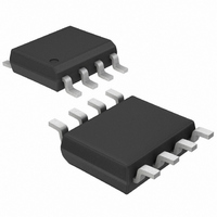
MAX4236BESA+ Maxim Integrated Products, MAX4236BESA+ Datasheet - Page 6

MAX4236BESA+
Manufacturer Part Number
MAX4236BESA+
Description
IC OP AMP R-R 8-SOIC
Manufacturer
Maxim Integrated Products
Datasheet
1.MAX4236BESA.pdf
(14 pages)
Specifications of MAX4236BESA+
Amplifier Type
General Purpose
Number Of Circuits
1
Output Type
Rail-to-Rail
Slew Rate
0.3 V/µs
Gain Bandwidth Product
1.7MHz
Current - Input Bias
1pA
Voltage - Input Offset
5µV
Current - Supply
350µA
Current - Output / Channel
30mA
Voltage - Supply, Single/dual (±)
2.4 V ~ 5.5 V, ±1.2 V ~ 2.75 V
Operating Temperature
-40°C ~ 85°C
Mounting Type
Surface Mount
Package / Case
8-SOIC (3.9mm Width)
Number Of Channels
1
Common Mode Rejection Ratio (min)
84 dB
Input Offset Voltage
0.05 mV
Input Bias Current (max)
500 pA
Operating Supply Voltage
3 V, 5 V
Maximum Power Dissipation
471 mW
Maximum Operating Temperature
+ 85 C
Minimum Operating Temperature
- 40 C
Mounting Style
SMD/SMT
Shutdown
Yes
Supply Voltage (max)
5.5 V
Supply Voltage (min)
2.4 V
Technology
BiCMOS
Voltage Gain Db
128 dB
Lead Free Status / RoHS Status
Lead free / RoHS Compliant
-3db Bandwidth
-
Lead Free Status / Rohs Status
Lead free / RoHS Compliant
SOT23, Very High Precision, 3V/5V
Rail-To-Rail Op Amps
ELECTRICAL CHARACTERISTICS (SOT23-6) (continued)
(V
values are at V
(V
6
Note 1: All devices are 100% production tested at T
Note 2: Guaranteed by design, not production tested.
Note 3: Maxim specification limits for the temperature coefficient of the offset voltage (TCV
Settling Time
Total Harmonic Distortion
Input Capacitance
Input Voltage Noise Density
Input Noise Voltage
Capacitive Load Stability
Shutdown Mode Output
Leakage
SHDN Logic Low
SHDN Logic High
SHDN Input Current
Shutdown Delay Time
Shutdown Recovery Time
CC
CC
_______________________________________________________________________________________
18
16
14
12
10
8
6
4
2
0
= +2.4V to +5.5V, V
= +5V, V
-10
unless otherwise specified.
pin SO and µMAX packages.
V
PARAMETER
CC
-8
= 5V
-6 -4
EE
CC
V
= 0, V
OS
= +5V and T
DISTRIBUTION
-2 0
V
OS
CM
( V)
EE
2
= V
= 0, V
4
CC
A
= +25°C.) (Note 1)
6
/2, R
CM
8 10
SYMBOL
I
OUT(SH)
C
L
e
THD
t
t
= 0, V
C
LOAD
V
(SH)
(EN)
np-p
V
e
= 100k to V
t
S
IN
IH
IL
n
OUT
V
f = 5kHz, V
R
f = 100kHz
f = 1kHz
f = 0.1Hz to 10Hz
No sustained oscillations
Device in shutdown mode (SHDN = V
V
SHDN = V
R
R
= V
OUT
OUT
L
L
L
25
20
15
10
5
0
= 10k
= 1k
= 1k
A
-2.0 -1.5 -1.0 -0.5
CC
CC
V
settling to within 0.01%
= 0 to V
= +25°C; all specifications over temperature are guaranteed by design,
CC
/2, T
/2, R
= 5V
EE
OUT
A
L
TCV
or V
CC
= +25°C, unless otherwise noted.)
= 100k
CONDITIONS
= 2Vp-p, V
OS
TCV
CC
DISTRIBUTION
OS
0
( V/ C)
Typical Operating Characteristics
to V
0.5 1.0 1.5
CC
CC
= +5V
/2, T
MAX4236
MAX4237
MAX4236
MAX4237
A
2.0
= T
EE
)
MIN
OS
to T
) are 100% tested for the A-grade, 8-
-20
-40
-60
-80
80
60
40
20
0.7 x V
0
MAX
-50
MIN
OFFSET VOLTAGE vs. TEMPERATURE
, unless otherwise noted. Typical
CC
-25
±0.01
0.001
0
TYP
200
200
TEMPERATURE ( C)
7.5
0.2
14
1
1
1
1
4
25
0.3 x V
50
MAX
±1.0
3
CC
75
nV/ Hz
UNITS
100
µVp-p
pF
µA
µA
µs
µs
µs
pF
V
V
%
125


