HTOP01 Honeywell Microelectronics & Precision Sensors, HTOP01 Datasheet - Page 2
HTOP01
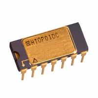
Manufacturer Part Number
HTOP01
Description
IC OP AMP DUAL HI TEMP 14-DIP
Manufacturer
Honeywell Microelectronics & Precision Sensors
Series
HTMOS™r
Datasheet
1.HTOP01.pdf
(6 pages)
Specifications of HTOP01
Amplifier Type
Chopper (Zero-Drift)
Number Of Circuits
2
Slew Rate
1.5 V/µs
Gain Bandwidth Product
2MHz
Current - Input Bias
10pA
Voltage - Input Offset
100µV
Current - Supply
5mA
Current - Output / Channel
20mA
Voltage - Supply, Single/dual (±)
4.5 V ~ 5.5 V
Operating Temperature
-55°C ~ 225°C
Mounting Type
Through Hole
Package / Case
14-CDIP (0.300", 7.62mm)
Lead Free Status / RoHS Status
Contains lead / RoHS non-compliant
Output Type
-
-3db Bandwidth
-
Other names
342-1081
Available stocks
Company
Part Number
Manufacturer
Quantity
Price


FUNCTIONAL BLOCK DIAGRAM
SHDN
SIGNAL DESCRIPTION
ABSOLUTE MAXIMUM RATINGS (1)
OUTA
XCLK
www.honeywell.com
INMA
INPA
VSS
VDD
Pin Name
SEL
XCLK
SHDN
INPA, INPB
INMA, INMB
OUTA, OUTB
VDD
VSS
No connect
Symbol
VDD
VPIN
TSTORE
IOUT
ESD
PJC
(1) Stresses in excess of those listed above may result in immediate permanent damage to the device. These are stress ratings only, and
(2) Voltage referenced to VSS.
(3) Class 2 Electrostatic Discharge (ESD) input protection voltage per MIL-STD-883, Method 3015
operation at these levels is not implied. Frequent or extended exposure to absolute maximum conditions may affect device reliability.
5
6
7
1
2
3
4
14 Pin DIP
Parameter
Supply Voltage (2)
Voltage on Any Pin (2)
Storage Temperature
Average Output Current
Electrostatic Discharge Protection Voltage (3)
Package Thermal Resistance
(Junction-to-Case)
HTOP01
Number
4, 11
1, 14
5,10
6,12
Pin
3, 9
13
2
7
8
10
14
13
12
11
9
8
Description
Digital input pin. Selects either internal clock (SEL=0) or externally applied clock
(SEL=1).
Digital input pin. External clock input. When SEL=1, XCLK is enabled, and the
internal ping-pong amplifier action occurs on each XCLK edge. When SEL=0, XCLK
is disabled. When not used, XCLK should be connected to VDD or VSS.
Digital input pin. Power Shutdown control input. When SHDN=1, all analog circuitry is
de-powered/disabled, and only leakage current will flow into VDD. When SHDN=0,
normal circuit operation occurs.
Non-inverting amplifier inputs for amplifier “A” and “B” respectively.
Inverting amplifier inputs for amplifier “A” and “B” respectively.
Amplifier “A” and “B” outputs.
Positive supply connection.
Negative supply connection.
Pin not used.
OUTB
SEL
VSS
INPB
INMB
VDD
No
connection
INM
INP
14 Pin DIP
V
V
Ref
Ref
1
2
C
C
A1,Ref
A2,Ref
2
1
1
2
-
+ +
-
+ +
A1
A2
1000
Min
-0.5
-0.5
-65
-
-
Rating
C
C
A1
A2
1
2
2
1
VDD+0.5
Max
15.0
300
6.5
50
Open
Closed
Output
1, 2
Stage
1
Units
Volts
Volts
°C
mA
V
°C/W
2
T=1/f
1
clk
OUT
2
t
2
Related parts for HTOP01
Image
Part Number
Description
Manufacturer
Datasheet
Request
R

Part Number:
Description:
MAGNETIC SENSORS
Manufacturer:
Honeywell Microelectronics & Precision Sensors

Part Number:
Description:
MAGNETIC SENSORS
Manufacturer:
Honeywell Microelectronics & Precision Sensors

Part Number:
Description:
MAGNETIC SENSORS
Manufacturer:
Honeywell Microelectronics & Precision Sensors
Part Number:
Description:
MAGNETIC SENSORS
Manufacturer:
Honeywell Microelectronics & Precision Sensors
Part Number:
Description:
MAGNETIC SENSORS
Manufacturer:
Honeywell Microelectronics & Precision Sensors
Datasheet:
Part Number:
Description:
MAGNETIC SENSORS
Manufacturer:
Honeywell Microelectronics & Precision Sensors

Part Number:
Description:
MAGNETIC SENSORS
Manufacturer:
Honeywell Microelectronics & Precision Sensors
Datasheet:

Part Number:
Description:
MAGNETIC SENSORS
Manufacturer:
Honeywell Microelectronics & Precision Sensors
Datasheet:

Part Number:
Description:
MAGNETIC SENSORS
Manufacturer:
Honeywell Microelectronics & Precision Sensors
Datasheet:
Part Number:
Description:
MAGNETIC SENSORS
Manufacturer:
Honeywell Microelectronics & Precision Sensors

Part Number:
Description:
SENSOR LINEAR MAGN 1 AXIS 8-SIP
Manufacturer:
Honeywell Microelectronics & Precision Sensors
Datasheet:

Part Number:
Description:
SENSOR MAGN 2 AXIS 10-MSOP
Manufacturer:
Honeywell Microelectronics & Precision Sensors
Datasheet:

Part Number:
Description:
Magnetic Sensor
Manufacturer:
Honeywell Microelectronics & Precision Sensors
Datasheet:

Part Number:
Description:
Magnetic Sensor
Manufacturer:
Honeywell Microelectronics & Precision Sensors
Datasheet:

Part Number:
Description:
IC, MAGNETO RESISTIVE SENSOR, LCC-16
Manufacturer:
Honeywell Microelectronics & Precision Sensors
Datasheet: