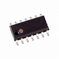
MCP6L04T-E/SL Microchip Technology, MCP6L04T-E/SL Datasheet - Page 3

MCP6L04T-E/SL
Manufacturer Part Number
MCP6L04T-E/SL
Description
IC OPAMP 1.0MHZ 1.8V 14-SOIC
Manufacturer
Microchip Technology
Datasheet
1.MCP6L02T-EMS.pdf
(32 pages)
Specifications of MCP6L04T-E/SL
Slew Rate
0.6 V/µs
Package / Case
14-SOIC (3.9mm Width), 14-SOL
Amplifier Type
General Purpose
Number Of Circuits
4
Output Type
Rail-to-Rail
Gain Bandwidth Product
1MHz
Current - Input Bias
2pA
Voltage - Input Offset
1000µV
Current - Supply
85µA
Current - Output / Channel
20mA
Voltage - Supply, Single/dual (±)
1.8 V ~ 6 V
Operating Temperature
-40°C ~ 125°C
Mounting Type
Surface Mount
Number Of Channels
4
Common Mode Rejection Ratio (min)
78 dB
Input Offset Voltage
5 mV
Input Bias Current (max)
2 pA
Operating Supply Voltage
3 V, 5 V
Maximum Operating Temperature
+ 125 C
Minimum Operating Temperature
- 40 C
Mounting Style
SMD/SMT
Shutdown
No
Supply Voltage (max)
6 V
Supply Voltage (min)
1.8 V
Technology
CMOS
Voltage Gain Db
105 dB
Lead Free Status / RoHS Status
Lead free / RoHS Compliant
-3db Bandwidth
-
Lead Free Status / Rohs Status
Lead free / RoHS Compliant
Other names
MCP6L04T-E/SLTR
Available stocks
Company
Part Number
Manufacturer
Quantity
Price
Company:
Part Number:
MCP6L04T-E/SL
Manufacturer:
Microchip
Quantity:
6 423
Part Number:
MCP6L04T-E/SL
Manufacturer:
MICROCHIP/微芯
Quantity:
20 000
1.0
1.1
V
Current at Input Pins ....................................................±2 mA
Analog Inputs (V
All Inputs and Outputs ................... V
Difference Input voltage ...................................... |V
Output Short Circuit Current ................................ Continuous
Current at Output and Supply Pins ..........................±150 mA
Storage Temperature ...................................-65°C to +150°C
Max. Junction Temperature ........................................ +150°C
ESD protection on all pins (HBM, MM) ................≥ 4 kV, 200V
1.2
TABLE 1-1:
© 2009 Microchip Technology Inc.
Electrical Characteristics: Unless otherwise indicated, T
V
Input Offset
Input Offset Voltage
Input Offset Voltage Drift
Power Supply Rejection Ratio
Input Current and Impedance
Input Bias Current
Input Offset Current
Common Mode Input Impedance
Differential Input Impedance
Common Mode
Common-Mode Input Voltage Range
Common-Mode Rejection Ratio
Open Loop Gain
DC Open Loop Gain (large signal)
Output
Maximum Output Voltage Swing
Output Short Circuit Current
Power Supply
Supply Voltage
Quiescent Current per Amplifier
Note 1:
DD
L
Across Temperature
Across Temperature
= V
– V
DD
SS
/2, and R
Absolute Maximum Ratings †
.......................................................................7.0V
Parameters
For design guidance only; not tested.
Specifications
ELECTRICAL CHARACTERISTICS
IN
+, V
L
DC ELECTRICAL SPECIFICATIONS
= 10 kΩ to V
IN
–) †† ....... V
L
(refer to
SS
SS
– 1.0V to V
– 0.3V to V
ΔV
CMRR
PSRR
Z
V
Sym
V
OS
Z
V
V
A
V
Figure
I
I
DIFF
CMR
I
I
I
I
OS
SC
CM
OS
OH
DD
OL
OL
Q
B
B
B
/ΔT
A
1-1).
DD
DD
DD
(Note 1)
+ 1.0V
+ 0.3V
4.965
– V
Min
-0.3
1.8
30
—
—
—
—
—
—
—
—
—
—
—
—
-5
SS
A
|
= +25°C, V
10
10
2,000
Typ
105
±20
±1
±2
83
80
±1
78
85
—
—
—
—
13
13
2
||5
||2
†
Maximum Ratings” may cause permanent damage to the
device. This is a stress rating only and functional operation of
the device at those or any other conditions above those
indicated in the operational listings of this specification is not
implied. Exposure to maximum rating conditions for extended
periods may affect device reliability.
†† See Section 4.1.2 “Input Voltage and Current Limits”.
DD
Notice: Stresses above those listed under “Absolute
MCP6L01/1R/1U/2/4
= 5.0V, V
(Note 1)
0.035
Max
170
5.3
6.0
+5
—
—
—
—
—
—
—
—
—
—
—
—
SS
= GND, V
Units
µV/°C T
Ω||pF
Ω||pF
mV
mA
µA
dB
pA
pA
pA
pA
dB
dB
V
V
V
V
CM
T
T
V
V
G = +2, 0.5V Input Overdrive
G = +2, 0.5V Input Overdrive
I
O
A
A
A
CM
OUT
= -40°C to+125°C
= +85°C
= +125°C
= 0
= V
= -0.3V to 5.3V
= 0.2V to 4.8V
SS
, V
Conditions
OUT
≈ V
DS22140A-page 3
DD
/2,


