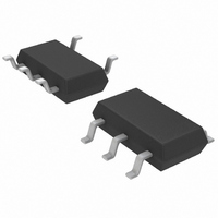
LT6220CS5#TRM Linear Technology, LT6220CS5#TRM Datasheet - Page 17

LT6220CS5#TRM
Manufacturer Part Number
LT6220CS5#TRM
Description
IC OPAMP PREC LP R-R TSOT23-5
Manufacturer
Linear Technology
Datasheet
1.LT6220CS5TRMPBF.pdf
(20 pages)
Specifications of LT6220CS5#TRM
Amplifier Type
General Purpose
Number Of Circuits
1
Output Type
Rail-to-Rail
Slew Rate
20 V/µs
Gain Bandwidth Product
60MHz
Current - Input Bias
250nA
Voltage - Input Offset
700µV
Current - Supply
1mA
Current - Output / Channel
50mA
Voltage - Supply, Single/dual (±)
2.2 V ~ 12.6 V, ±1.1 V ~ 6.3 V
Operating Temperature
0°C ~ 70°C
Mounting Type
Surface Mount
Package / Case
TSOT-23-5, TSOT-5, TSOP-5
Lead Free Status / RoHS Status
Contains lead / RoHS non-compliant
-3db Bandwidth
-
Other names
LT6220CS5#TRMTR
Available stocks
Company
Part Number
Manufacturer
Quantity
Price
PACKAGE DESCRIPTIO
and the output of the lower path is:
Note that the input common mode voltage does not appear
in the output as either a common mode or a difference
mode term. However the voltage V
output terms, and with the same polarity, so it sets up the
output DC level. Also, the differential input voltage V
appears fully at both outputs with opposite polarity, giving
3.5 ±0.05
PACKAGE DESCRIPTIO
+OUT = 3 • (2/3 • V
2.15 ±0.05
• (V
= 2V
= V
RECOMMENDED SOLDER PAD PITCH AND DIMENSIONS
1.65 ±0.05
(2 SIDES)
ICM
0.25 ± 0.05
OCM
ICM
– V
+ V
+ V
DIFF
DIFF
OCM
ICM
/2)
2.38 ±0.05
(2 SIDES)
– 2V
+ 1/3 • V
0.50
BSC
ICM
+ V
OCM
OCM
0.675 ±0.05
DIFF
U
U
does appear in the
) – 2
PACKAGE
OUTLINE
8-Lead Plastic DFN (3mm × 3mm)
(Reference LTC DWG # 05-08-1698)
TOP MARK
(NOTE 6)
PIN 1
0.200 REF
DIFF
DD Package
NOTE:
1. DRAWING TO BE MADE A JEDEC PACKAGE OUTLINE M0-229 VARIATION OF (WEED-1)
2. DRAWING NOT TO SCALE
3. ALL DIMENSIONS ARE IN MILLIMETERS
4. DIMENSIONS OF EXPOSED PAD ON BOTTOM OF PACKAGE DO NOT INCLUDE
5. EXPOSED PAD SHALL BE SOLDER PLATED
6. SHADED AREA IS ONLY A REFERENCE FOR PIN 1 LOCATION
MOLD FLASH. MOLD FLASH, IF PRESENT, SHALL NOT EXCEED 0.15mm ON ANY SIDE
ON TOP AND BOTTOM OF PACKAGE
rise to the effective differential gain of 2. Calculations show
that using 1% resistors gives worst-case input common
mode feedthrough better than –31dB, whether looking at
the output common mode or difference mode. Consider-
ing the 6dB of gain, worst-case common mode rejection
ratio is 37dB. (Remember this is assuming 1% resistors.
Of course, this can be improved with more precise resis-
tors.) Results achieved on the bench with typical 1%
resistors showed 67dB of CMRR at low frequency and
40dB CMRR at 1MHz. Gains other than 2 can be achieved
by setting R3 = α • (R1||R2), R5 = α • R4 and R7 = α • R6
where gain = α.
LT6220/LT6221/LT6222
0.75 ±0.05
3.00 ±0.10
(4 SIDES)
0.00 – 0.05
1.65 ± 0.10
(2 SIDES)
BOTTOM VIEW—EXPOSED PAD
0.25 ± 0.05
R = 0.115
TYP
4
5
2.38 ±0.10
(2 SIDES)
8
1
0.50 BSC
0.38 ± 0.10
17
622012fa
(DD8) DFN 1203


