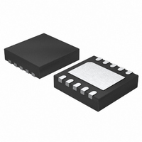
LTC6078IDD Linear Technology, LTC6078IDD Datasheet

LTC6078IDD
Specifications of LTC6078IDD
Available stocks
Related parts for LTC6078IDD
LTC6078IDD Summary of contents
Page 1
... LTC6078 is available in 8-lead MSOP and 10-lead DFN packages. The quad amplifi er LTC6079 is available in 16-lead SSOP and DFN packages. , LT, LTC and LTM are registered trademarks of Linear Technology Corporation. All other trademarks are the property of their respective owners. Patent Pending. 5V ...
Page 2
... OUTC PACKAGE 16-LEAD PLASTIC SSOP T = 150°C, θ = 110°C/W JMAX JA ORDER PART DD PART NUMBER MARKING* LTC6078CDD LBBB LTC6078IDD LBBB ORDER PART MS8 PART NUMBER MARKING* LTAJZ LTAJZ LTAJZ LTAJZ LTAJZ LTAJZ ORDER PART DHC PART NUMBER MARKING* 6079 6079 ORDER PART ...
Page 3
ELECTRICAL CHARACTERISTICS temperature range, otherwise specifi cations are at T SYMBOL PARAMETER CONDITIONS V Offset Voltage (Note 5) LTC6078MS8, LTC6078AMS8, LTC6079GN OS LTC6078DD, LTC6079DHC LTC6078AMS8 LTC6078MS8 LTC6079GN LTC6078DD LTC6079DHC ΔV ⁄ΔT Input Offset Voltage Drift LTC6078AMS8 OS (Note 5) LTC6078MS8 ...
Page 4
LTC6078/LTC6079 ELECTRICAL CHARACTERISTICS temperature range, otherwise specifi cations are at T SYMBOL PARAMETER CONDITIONS I Supply Current No Load S (per Amplifi er) Shutdown Current Shutdown, V (per Amplifi er) V Supply Voltage Range Guaranteed by the PSRR Test S ...
Page 5
ELECTRICAL CHARACTERISTICS temperature range, otherwise specifi cations are at T SYMBOL PARAMETER CONDITIONS CMRR Common Mode Rejection All Packages Ratio LTC6078AMS8 LTC6078AMS8 LTC6078MS8 LTC6078MS8 LTC6079GN LTC6079GN LTC6078DD, LTC6079DHC LTC6078DD, LTC6079DHC PSRR Power Supply Rejection Ratio V = 2.7V to 5.5V ...
Page 6
LTC6078/LTC6079 W U TYPICAL PERFOR A CE CHARACTERISTICS V Distribution OS 14 LTC6078MS8 0. 25° –11 –9 –7 –5 –3 – ...
Page 7
W U TYPICAL PERFOR A CE CHARACTERISTICS Output Voltage Swing vs Load Current + –0.5 S SOURCE +V –1 –1 –2 0.7V CM –V +2.0 S –V ...
Page 8
LTC6078/LTC6079 W U TYPICAL PERFOR A CE CHARACTERISTICS Disabled Output Impedence vs Frequency 1000 0. 25°C A 100 0.1 0.01 100 1k 10k 100k 1M ...
Page 9
U U APPLICATIO S I FOR ATIO Preserving Input Precision Preserving input accuracy of the LTC6078/LTC6079 re- quires that the application circuit and PC board layout do not introduce errors comparable or greater than the 10µV typical offset of the ...
Page 10
LTC6078/LTC6079 U U APPLICATIO S I FOR ATIO PC Board Layout Mechanical stress board and soldering-induced stress can cause the V and and DHC packages are more sensitive to stress. A simple way to ...
Page 11
U TYPICAL APPLICATIO COLUMBIA RESEARCH LABS 3021 ACCELERATOR 2.7V High Side Current Sense 1/2 2N7002 LTC6078 – V OUT LOAD • ...
Page 12
LTC6078/LTC6079 U TYPICAL APPLICATIO 1µF V SUP IN 5.2V TO 20V LT1761-5 1µF SHDN BAT54S V DD 100k LTC6906 499k V OUT DD 0.1µF GRD GND V SET DIV ...
Page 13
U TYPICAL APPLICATIO 1.8V TO 20V 10µF 0 ≤ I ≤ 1.5A LOAD 1.22V ≤ V ≤ V OUT DD LDO LOADS MATCH TO WITHIN 1mA WITH 10mΩ OF BALLAST RESISTANCE (2 INCHES OF AWG 28 ...
Page 14
LTC6078/LTC6079 U TYPICAL APPLICATIO LT1634 0.01µF 1.25V 3200Ω YSI #44201 THERMOLINEAR NETWORK 6250Ω – LTC6078 Thermistor Amplifi er with Overtemperature Alarm 29.4k 71.5k 200k + – + ...
Page 15
U TYPICAL APPLICATIO S Precision Voltage-Controlled Current Source 1/2 LTC6078 V – OUT R SET I < 0. ERROR 0.68µ SET 1µF 1µ ...
Page 16
LTC6078/LTC6079 PACKAGE DESCRIPTIO 3.50 ±0.05 1.65 ±0.05 2.15 ±0.05 (2 SIDES) 0.25 ± 0.05 RECOMMENDED SOLDER PAD PITCH AND DIMENSIONS PIN 1 TOP MARK (SEE NOTE 6) 0.200 REF NOTE: 1. DRAWING TO BE MADE A JEDEC PACKAGE OUTLINE M0-229 ...
Page 17
PACKAGE DESCRIPTIO 3.50 ±0.05 1.65 ±0.05 2.20 ±0.05 (2 SIDES) RECOMMENDED SOLDER PAD PITCH AND DIMENSIONS PIN 1 TOP MARK (SEE NOTE 6) 0.200 REF NOTE: 1. DRAWING PROPOSED TO BE MADE VARIATION OF VERSION (WJED-1) IN JEDEC PACKAGE OUTLINE ...
Page 18
LTC6078/LTC6079 PACKAGE DESCRIPTIO 5.23 (.206) MIN 0.42 ± 0.038 (.0165 ± .0015) TYP RECOMMENDED SOLDER PAD LAYOUT 0.254 (.010) GAUGE PLANE 0.18 (.007) NOTE: 1. DIMENSIONS IN MILLIMETER/(INCH) 2. DRAWING NOT TO SCALE 3. DIMENSION DOES NOT INCLUDE MOLD FLASH, ...
Page 19
... FLASH SHALL NOT EXCEED 0.010" (0.254mm) PER SIDE Information furnished by Linear Technology Corporation is believed to be accurate and reliable. However, no responsibility is assumed for its use. Linear Technology Corporation makes no representa- tion that the interconnection of its circuits as described herein will not infringe on existing patent rights. ...
Page 20
... CIRCUIT BW ≈ 1.25MHz e = 2.6nV/√Hz (RTI) AT 1kHz n CIRCUIT V = 25µV (MAX) RTI OS COMMENTS 3µ 30nV/°C V Drift OS OS 60µ 300pA 135µ www.linear.com ● LT1226 V OUT – 10k 10k 10Ω 60789 TA06 LT 0506 REV A • PRINTED IN USA © LINEAR TECHNOLOGY CORPORATION 2005 60789fa ...


