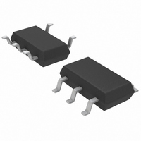
LT1880CS5#TRM Linear Technology, LT1880CS5#TRM Datasheet - Page 8

LT1880CS5#TRM
Manufacturer Part Number
LT1880CS5#TRM
Description
IC OPAMP PICO/IN RR/OUT TSOT23-5
Manufacturer
Linear Technology
Datasheet
1.LT1880CS5TRM.pdf
(12 pages)
Specifications of LT1880CS5#TRM
Amplifier Type
General Purpose
Number Of Circuits
1
Output Type
Rail-to-Rail
Slew Rate
0.55 V/µs
Gain Bandwidth Product
1.1MHz
Current - Input Bias
150pA
Voltage - Input Offset
40µV
Current - Supply
1.5mA
Current - Output / Channel
25mA
Voltage - Supply, Single/dual (±)
2.7 V ~ 36 V, ±1.35 V ~ 18 V
Operating Temperature
0°C ~ 70°C
Mounting Type
Surface Mount
Package / Case
TSOT-23-5, TSOT-5, TSOP-5
Lead Free Status / RoHS Status
Contains lead / RoHS non-compliant
-3db Bandwidth
-
Other names
LT1880CS5#TRMTR
Available stocks
Company
Part Number
Manufacturer
Quantity
Price
APPLICATIONS INFORMATION
LT1880
The LT1880 single op amp features exceptional input
precision with rail-to-rail output swing. Slew rate and small
signal bandwidth are superior to other amplifi ers with
comparable input precision. These characteristics make
the LT1880 a convenient choice for precision low voltage
systems and for improved AC performance in higher voltage
precision systems. Obtaining benefi cial advantage of the
precision inherent in the amplifi er depends upon proper
applications circuit design and board layout.
Preserving Input Precision
Preserving the input voltage accuracy of the LT1880
requires that the applications circuit and PC board layout
do not introduce errors comparable to or greater than the
40μV offset. Temperature differentials across the input
connections can generate thermocouple voltages of 10’s
of microvolts. PC board layouts should keep connections
to the amplifi er’s input pins close together and away from
heat dissipating components. Air currents across the board
can also generate temperature differentials.
The extremely low input bias currents, 150pA, allow high
accuracy to be maintained with high impedance sources and
feedback networks. The LT1880’s low input bias currents
are obtained by using a cancellation circuit on-chip. This
causes the resulting I
implied by the l
The user should not try to balance the input resistances in
each input lead, as is commonly recommended with most
amplifi ers. The impedance at either input should be kept
as small as possible to minimize total circuit error.
PC board layout is important to insure that leakage currents
do not corrupt the low I
precision, high impedance circuits, the input pins should
be surrounded by a guard ring of PC board interconnect,
with the guard driven to the same common mode voltage
as the amplifi er inputs.
Input Common Mode Range
The LT1880 output is able to swing nearly to each power
supply rail, but the input stage is limited to operating
between V
mode range will cause the gain to drop to zero, however
no gain reversal will occur.
8
–
+ 1V and V
OS
specifi cation being comparable to I
BIAS
+
+
– 1.2V. Exceeding this common
and I
BIAS
BIAS
of the amplifi er. In high
–
to be uncorrelated, as
BIAS
.
Input Protection
The inverting and noninverting input pins of the LT1880
have limited on-chip protection. ESD protection is provided
to prevent damage during handling. The input transistors
have voltage clamping and limiting resistors to protect
against input differentials up to 10V. Short transients
above this level will also be tolerated. If the input pins can
see a sustained differential voltage above 10V, external
limiting resistors should be used to prevent damage to
the amplifi er. A 1k resistor in each input lead will provide
protection against a 30V differential voltage.
Capacitive Loads
The LT1880 can drive capacitive loads up to 600pF in unity
gain. The capacitive load driving capability increases as
the amplifi er is used in higher gain confi gurations, see the
graph labled Capacitive Load Response. Capacitive load
driving may be increased by decoupling the capacitance
from the output with a small resistance.
Getting Rail-to-Rail Operation without Rail-to-Rail
Inputs
The LT1880 does not have rail-to-rail inputs, but for most
inverting applications and noninverting gain applications,
this is largely inconsequential. Figure 1 shows the basic
op amp configurations, what happens to the op amp
inputs, and whether or not the op amp must have rail-
to-rail inputs.
30
25
20
15
10
5
0
10
Capacitance Load Response
V
T
S
A
= 25°C
= ±15V
CAPACITIVE LOAD (pF)
100
A
V
A
= 10
V
= 1
1000
1880 G25
10000
1880fa


