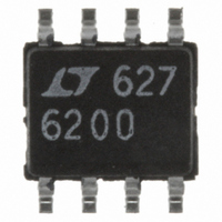
LT6200CS8#TRPBF Linear Technology, LT6200CS8#TRPBF Datasheet - Page 5

LT6200CS8#TRPBF
Manufacturer Part Number
LT6200CS8#TRPBF
Description
IC OPAMP R-R I/O 165MHZ 8-SOIC
Manufacturer
Linear Technology
Datasheet
1.LT6200CS6TRMPBF.pdf
(26 pages)
Specifications of LT6200CS8#TRPBF
Amplifier Type
Buffer
Number Of Circuits
1
Output Type
Rail-to-Rail
Slew Rate
50 V/µs
Gain Bandwidth Product
165MHz
Current - Input Bias
23µA
Voltage - Input Offset
2500µV
Current - Supply
20mA
Current - Output / Channel
90mA
Voltage - Supply, Single/dual (±)
2.5 V ~ 12.6 V, ±1.25 V ~ 6.3 V
Operating Temperature
0°C ~ 70°C
Mounting Type
Surface Mount
Package / Case
8-SOIC (3.9mm Width)
Lead Free Status / RoHS Status
Lead free / RoHS Compliant
-3db Bandwidth
-
Available stocks
Company
Part Number
Manufacturer
Quantity
Price
ELECTRICAL CHARACTERISTICS
temperature range. V
SYMBOL
A
CMRR
PSRR
V
V
I
I
I
V
V
t
t
SR
FPBW
The
V
SYMBOL
V
V
I
SC
S
SHDN
ON
OFF
B
VOL
OL
OH
L
H
S
OS
OS
= 5V, 0V; V
TC
●
denotes the specifi cations which apply over –40°C < T
PARAMETER
Input Offset Voltage
Input Offset Voltage Match
(Channel-to-Channel) (Note 11)
Input Offset Voltage Drift (Note 8)
Input Bias Current
PARAMETER
Large-Signal Gain
Common Mode Rejection Ratio
CMRR Match (Channel-to-Channel) (Note 11)
Power Supply Rejection Ratio
PSRR Match (Channel-to-Channel) (Note 11)
Minimum Supply Voltage (Note 6)
Output Voltage Swing LOW (Note 7)
Output Voltage Swing HIGH (Note 7)
Short-Circuit Current
Supply Current per Amplifi er
Disabled Supply Current per Amplifi er
SHDN Pin Current
V
V
Shutdown Output Leakage Current
Turn-On Time
Turn-Off Time
Slew Rate
Full Power Bandwidth (Note 9)
SHDN
SHDN
S
= 3V, 0V; V
Pin Input Voltage LOW
Pin Input Voltage HIGH
S
= 5V, 0V; V
CM
= V
OUT
S
= 3V, 0V; V
= half supply, V
CM
= V
SHDN
OUT
CONDITIONS
V
V
V
V
V
V
V
V
V
V
CONDITIONS
V
V
V
V
V
V
V
V
V
No Load
I
V
V
No Load
I
V
V
V
V
V
V
V
V
V
V
V
V
A
LT6200-5
LT6200-10
V
S
S
S
S
CM
CM
CM
CM
CM
CM
SINK
SOURCE
S
S
S
S
S
S
S
S
S
S
S
S
S
S
S
S
S
SHDN
SHDN
SHDN
SHDN
SHDN
S
V
S
= 5V, V
= 3V, V
= 5V, V
= 3V, V
= half supply, V
= 5V, V
= 5V, V
= 3V, V
= 5V, V
= 5V, V
= 3V, V
= 3V to 10V, LT6201DD V
= 5V
= –10, R
= 5V, V
= 3V to 10V, LT6201DD V
= 5V, I
= 3V, I
= 5V, I
= 3V, I
= 3V
= 5V
= 3V
= 5V, A
= 5V, V
= Half Supply
= Half Supply
= V
= V
= OPEN, unless otherwise noted. (Note 5)
= Half Supply
= V
The
= 5mA
A
+
–
= 0.3V
= 0.3V
= 0.3V
= 0.3V to 4.5V, R
= 4.5V to 0.3V, R
–
< 85°C temperature range. Excludes the LT6201 in the DD package (Note 3).
= 5mA
to V
CM
CM
CM
CM
●
SINK
SINK
SOURCE
SOURCE
O
O
O
CM
CM
CM
CM
V
OUT
denotes the specifi cations which apply over 0°C < T
L
= 0.5V to 4.5V,R
= 1.5V to 3.5V,R
= 0.5V to 2.5V,R
= –1, R
= Half Supply
= Half Supply
= V
= V
+
= 1k, V
= V
= 1.5V to 3.5V
= V
= 1.5V to 3.5V
= 20mA
= 20mA
= 3V
+
+
–
–
= 20mA
= 20mA
to V
to V
P-P
to V
to V
L
SHDN
O
= 1k, V
–
–
= 4V
(LT6200)
+
+
L
L
= 100Ω, V
= 100Ω, V
= OPEN, unless otherwise noted.
O
L
L
L
S
S
= 1k to V
= 100Ω to V
= 1k to V
= 4V
= 3V to 7V
= 3V to 7V
S
S
= 5V
= 5V
S
S
/2
/2
S
/2
LT6200-10/LT6201
LT6200/LT6200-5
l
l
l
l
l
l
l
l
l
l
l
l
l
l
l
l
l
l
l
l
l
l
l
l
l
l
l
l
l
l
l
l
l
l
l
l
l
l
l
l
l
l
l
V
MIN
+
3.07
±60
±45
7.5
46
13
64
80
60
80
60
60
29
–0.5
MIN
3
–40
–50
1.35
4.45
TYP
105
105
100
170
170
115
260
270
±90
±75
215
130
180
190
310
0.1
80
13
22
88
83
65
12
55
65
20
19
42
TYP
–10
–23
0.2
0.3
1.5
0.2
0.4
2.5
1
8
A
< 70°C
MAX
MAX
110
310
310
120
210
440
490
295
1.5
2.8
3.5
4.3
1.8
0.3
18
60
23
22
75
2
3
8
UNITS
UNITS
62001fd
V/mV
V/mV
V/mV
μV/ºC
5
V/μs
V/μs
V/μs
MHz
mV
mV
mV
mV
mV
mV
mV
mV
mV
mV
mV
mV
mV
mV
mA
mA
mA
mA
mA
μA
μA
μA
dB
dB
dB
dB
dB
dB
μA
μA
ns
ns
V
V
V


