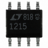
LT1215CS8 Linear Technology, LT1215CS8 Datasheet

LT1215CS8
Specifications of LT1215CS8
Available stocks
Related parts for LT1215CS8
LT1215CS8 Summary of contents
Page 1
... Full-Scale 12-Bit Systems: V 10V Full-Scale 16-Bit Systems: V Active Filters Photo Diode Amplifiers DAC Current to Voltage Amplifiers Battery-Powered Systems , LTC and LT are registered trademarks of Linear Technology Corporation. NOTE: 0.1% RESISTORS GIVE CMRR 68dB. GAIN IS 10.0V/V. COMMON MODE INPUT RANGE IS FROM 0.3V TO 3.0V. ...
Page 2
... JMAX LT1215AMJ8 ORDER PART NUMBER OUT A 1 – LT1216CN + + – OUT 16-LEAD PLASTIC 150 C, JMAX ORDER PART NUMBER TOP VIEW LT1215CS8 + 8 V OUT – + PART MARKING S8 PACKAGE 1215 = 150 C/W JA ORDER PART TOP VIEW NUMBER 16 OUT D 15 – LT1216CS 14 +IN D – ...
Page 3
... V = 100mV V O 0.01 0mA 10MHz 20Hz to 20kHz V O RMS LT1215/LT1216 PACKAGE PLASTIC DIP SURFACE MOUNT (N) LT1215ACN8 LT1215CN8 LT1215CS8 LT1216CN LT1216CS = 0.5V unless otherwise noted. OUT A LT1215AC LT1215C/LT1215M LT1215AM LT1216C TYP MAX MIN TYP MAX 125 300 150 450 0.8 1 120 420 ...
Page 4
LT1215/LT1216 5V ELECTRICAL C HARA TERISTICS 0.5V 0.5V OUT SYMBOL PARAMETER V Input Offset Voltage OS V Input Offset Voltage Drift OS (Note Input Offset ...
Page 5
ELECTRICAL C HARA TERISTICS 0.5V 0.5V, – OUT SYMBOL PARAMETER V Input Offset Voltage OS V Input Offset Voltage Drift OS (Note Input Offset ...
Page 6
LT1215/LT1216 + – 15V ELECTRICAL C HARA TERISTICS V = 15V 0V 0V OUT SYMBOL PARAMETER V Input Offset Voltage OS V Input Offset Voltage Drift OS (Note ...
Page 7
ELECTRICAL C HARA TERISTICS V = 3.3V 0.5V 0.5V OUT A SYMBOL PARAMETER CONDITIONS V Input Offset Voltage OS Input Voltage Range (Note 10) Maximum Output Voltage Swing Output High, No Load ...
Page 8
... INPUT OFFSET VOLTAGE ( V) 1215/16 G07 8 LT1215MJ8, LT1215AMJ8: LT1215CN8, LT1215ACN8: LT1215CS8: LT1216CN: LT1216CS: Note 6: This parameter is not 100% tested. Note 7: Guaranteed by correlation to 3.3V and 15V tests. Note 8: Slew rate is measured between 8. output swing of 10V on 15V supplies. Note 9: Most LT1215/LT1216 electrical characteristics change very little with supply voltage ...
Page 9
W U TYPICAL PERFOR A Voltage Gain vs Frequency 140 C = 20pF L 120 100 ±15V – 100 1k 10k 100k ...
Page 10
LT1215/LT1216 W U TYPICAL PERFOR A Open-Loop Voltage Gain vs Supply Voltage –55° 25° 125° ...
Page 11
W U TYPICAL PERFOR A 5V Small-Signal Response 50ns/DIV 1215/16 G34 V 15V Small-Signal Response 50ns/DIV V = 15V 1215/16 G34 5V Settling 50ns/DIV ...
Page 12
LT1215/LT1216 W U TYPICAL PERFOR A Supply Current vs Supply Voltage 6.5 6 125°C A 5.5 5 25°C A 4.5 4 –55°C A 3.5 3.0 2.5 2 SUPPLY VOLTAGE ...
Page 13
... The maximum ambient 125 C depending on the part rating. 2. The load is 500 , includes the feedback resistors. 3. The output can be anywhere between the supplies. PART LT1215MJ8 LT1215CN8 LT1215CS8 LT1216CN LT1216CS LT1215/LT1216 • – • ...
Page 14
LT1215/LT1216 PPLICATI S I FOR ATIO Inputs Typically at room temperature, the inputs of the LT1215/ LT1216 can common mode 400mV below ground (V and to within 1.5V of the positive supply with the amplifier still ...
Page 15
PPLICATI S I FOR ATIO Comparator Applications Sometimes it is desirable to use an op amp as a compara- tor. When operating the LT1215/LT1216 on a single 3. supply, the output interfaces directly with ...
Page 16
LT1215/LT1216 U TYPICAL APPLICATIO Single Supply, AC Coupled Input, RMS Calibrated, Average Detector BIASED DIFFERENTIAL SIGNAL 5V 20k + 10k LT1216 – 11.3k 22pF + LT1216 1k – V ...
Page 17
PACKAGE DESCRIPTIO CORNER LEADS OPTION 0.045 – 0.068 (1.143 – 1.727) FULL LEAD OPTION 0.300 BSC (0.762 BSC) 0.008 – 0.018 (0.203 – 0.457) NOTE: LEAD DIMENSIONS APPLY TO SOLDER DIP/PLATE OR TIN PLATE LEADS U J8 Package 8-Lead CERDIP ...
Page 18
LT1215/LT1216 PACKAGE DESCRIPTIO 0.300 – 0.325 (7.620 – 8.255) 0.009 – 0.015 (0.229 – 0.381) +0.035 0.325 –0.015 +0.889 8.255 –0.381 *THESE DIMENSIONS DO NOT INCLUDE MOLD FLASH OR PROTRUSIONS. MOLD FLASH OR PROTRUSIONS SHALL NOT EXCEED 0.010 INCH (0.254mm) ...
Page 19
... FLASH SHALL NOT EXCEED 0.010" (0.254mm) PER SIDE Information furnished by Linear Technology Corporation is believed to be accurate and reliable. However, no responsibility is assumed for its use. Linear Technology Corporation makes no represen- tation that the interconnection of its circuits as described herein will not infringe on existing patent rights. ...
Page 20
... Dual and Quad 12MHz, 400V Amps LT1358/LT1359 Dual and Quad 25MHz, 600V Amps LT1361/LT1362 Dual and Quad 50MHz, 800V Amps C-Load is a trademark of Linear Technology Corporation. Linear Technology Corporation 20 1630 McCarthy Blvd., Milpitas, CA 95035-7417 (408) 432-1900 FAX: (408) 434-0507 LT1216 Photo Diode Amplifier ...


