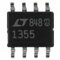
LT1355CS8 Linear Technology, LT1355CS8 Datasheet - Page 10

LT1355CS8
Manufacturer Part Number
LT1355CS8
Description
IC OP-AMP HISPD 12MHZ DUAL 8SOIC
Manufacturer
Linear Technology
Series
C-Load™r
Datasheet
1.LT1355CN8PBF.pdf
(16 pages)
Specifications of LT1355CS8
Amplifier Type
Voltage Feedback
Number Of Circuits
2
Slew Rate
400 V/µs
Gain Bandwidth Product
12MHz
Current - Input Bias
80nA
Voltage - Input Offset
300µV
Current - Supply
1mA
Current - Output / Channel
30mA
Voltage - Supply, Single/dual (±)
±2.5 V ~ 15 V
Operating Temperature
0°C ~ 70°C
Mounting Type
Surface Mount
Package / Case
8-SOIC (3.9mm Width)
Lead Free Status / RoHS Status
Contains lead / RoHS non-compliant
Output Type
-
-3db Bandwidth
-
Available stocks
Company
Part Number
Manufacturer
Quantity
Price
Part Number:
LT1355CS8
Manufacturer:
LT
Quantity:
20 000
Company:
Part Number:
LT1355CS8#PBF
Manufacturer:
LINEAR
Quantity:
29
Part Number:
LT1355CS8#TRPBF
Manufacturer:
LT
Quantity:
20 000
APPLICATIONS INFORMATION
Layout and Passive Components
The LT1355/LT1356 amplifi ers are easy to use and tolerant
of less than ideal layouts. For maximum performance (for
example, fast 0.01% settling) use a ground plane, short
lead lengths, and RF-quality bypass capacitors (0.01μF to
0.1μF). For high drive current applications use low ESR
bypass capacitors (1μF to 10μF tantalum).
The parallel combination of the feedback resistor and gain
setting resistor on the inverting input combine with the
input capacitance to form a pole which can cause peaking
or oscillations. If feedback resistors greater than 5k are
used, a parallel capacitor of value:
should be used to cancel the input pole and optimize
dynamic performance. For unity-gain applications where
a large feedback resistor is used, C
than or equal to C
Capacitive Loading
The LT1355/LT1356 are stable with any capacitive load.
As the capacitive load increases, both the bandwidth and
phase margin decrease so there will be peaking in the
frequency domain and in the transient response. Coaxial
cable can be driven directly, but for best pulse fi delity a
resistor of value equal to the characteristic impedance of
the cable (i.e., 75Ω) should be placed in series with the
output. The other end of the cable should be terminated
with the same value resistor to ground.
Input Considerations
Each of the LT1355/LT1356 inputs is the base of an NPN
and a PNP transistor whose base currents are of opposite
polarity and provide fi rst-order bias current cancellation.
Because of variation in the matching of NPN and PNP beta,
the polarity of the input bias current can be positive or
negative. The offset current does not depend on NPN/PNP
beta matching and is well controlled. The use of balanced
source resistance at each input is recommended for ap-
plications where DC accuracy must be maximized.
LT1355/LT1356
10
C
F
> R
G
x C
IN
/R
IN
F
.
F
should be greater
The inputs can withstand transient differential input volt-
ages up to 10V without damage and need no clamping
or source resistance for protection. Differential inputs,
however, generate large supply currents (tens of mA) as
required for high slew rates. If the device is used with
sustained differential inputs, the average supply current will
increase, excessive power dissipation will result and the
part may be damaged. The part should not be used as a
comparator, peak detector or other open-loop application
with large, sustained differential inputs. Under normal,
closed-loop operation, an increase of power dissipation is
only noticeable in applications with large slewing outputs
and is proportional to the magnitude of the differential input
voltage and the percent of the time that the inputs are apart.
Measure the average supply current for the application in
order to calculate the power dissipation.
Circuit Operation
The LT1355/LT1356 circuit topology is a true voltage
feedback amplifi er that has the slewing behavior of a cur-
rent feedback amplifi er. The operation of the circuit can
be understood by referring to the simplifi ed schematic.
The inputs are buffered by complementary NPN and
PNP emitter followers which drive an 800Ω resistor.
The input voltage appears across the resistor generating
currents which are mirrored into the high impedance
node. Complementary followers form an output stage
which buffers the gain node from the load. The bandwidth
is set by the input resistor and the capacitance on the
high impedance node. The slew rate is determined by the
current available to charge the gain node capacitance.
This current is the differential input voltage divided by
R1, so the slew rate is proportional to the input. Highest
slew rates are therefore seen in the lowest gain confi gura-
tions. For example, a 10V output step in a gain of 10 has
only a 1V input step, whereas the same output step in
unity gain has a 10 times greater input step. The curve of
Slew Rate vs Input Level illustrates this relationship. The
LT1355/LT1356 are tested for slew rate in a gain of –2 so
higher slew rates can be expected in gains of 1 and –1,
and lower slew rates in higher gain confi gurations.
13556fb


