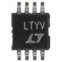
LTC1992-2CMS8 Linear Technology, LTC1992-2CMS8 Datasheet - Page 6

LTC1992-2CMS8
Manufacturer Part Number
LTC1992-2CMS8
Description
IC AMP/DVR I/O GAIN OF 2 8MSOP
Manufacturer
Linear Technology
Datasheet
1.LTC1992CMS8PBF.pdf
(42 pages)
Specifications of LTC1992-2CMS8
Amplifier Type
Differential
Number Of Circuits
1
Output Type
Differential, Rail-to-Rail
Slew Rate
1.5 V/µs
Gain Bandwidth Product
3.2MHz
Current - Input Bias
2pA
Voltage - Input Offset
250µV
Current - Supply
700µA
Current - Output / Channel
30mA
Voltage - Supply, Single/dual (±)
2.7 V ~ 11 V, ±1.35 V ~ 5.5 V
Operating Temperature
0°C ~ 70°C
Mounting Type
Surface Mount
Package / Case
8-MSOP, Micro8™, 8-uMAX, 8-uSOP,
Lead Free Status / RoHS Status
Contains lead / RoHS non-compliant
-3db Bandwidth
-
Available stocks
Company
Part Number
Manufacturer
Quantity
Price
Company:
Part Number:
LTC1992-2CMS8
Manufacturer:
LT
Quantity:
10 000
Part Number:
LTC1992-2CMS8
Manufacturer:
LINEAR/凌特
Quantity:
20 000
Company:
Part Number:
LTC1992-2CMS8#PBF
Manufacturer:
LT
Quantity:
759
elecTrical characTerisTics
LTC1992 Family
temperature range, otherwise specifications are at T
noted. V
defined as (+V
LTC1992-5 only.
SYMBOL PARAMETER
G
e
R
V
CMRR
SR
GBW
The
+V
as (+V
Typical values are at T
SYMBOL PARAMETER
G
e
R
V
CMRR
SR
GBW
Note 1: Stresses beyond those listed under Absolute Maximum Ratings
may cause permanent damage to the device. Exposure to any Absolute
Maximum Rating condition for extended periods may affect device
reliability and lifetime.
Note 2: Output load is connected to the midpoint of the +V
potentials. Measurement is taken single-ended, one output loaded at a
time.
Note 3: A heat sink may be required to keep the junction temperature
below the absolute maximum when the output is shorted indefinitely.
Note 4: Differential output slew rate. Slew rate is measured single ended
and doubled to get the listed numbers.
Note 5: The LTC1992C/LTC1992-XC/LTC1992I/LTC1992-XI are guaranteed
functional over an operating temperature of –40°C to 85°C. The
n
n
DIFF
IN
INCMR
DIFF
IN
INCMR
S
l
= 5V, –V
denotes the specifications which apply over the full operating temperature range, otherwise specifications are at T
OUT
OCM
Differential Gain
Differential Gain Error
Differential Gain Nonlinearity
Differential Gain Temperature Coefficient
Input Referred Noise Voltage Density (Note 7) f = 1kHz
Input Resistance, Single-Ended +IN, –IN Pins
Input Signal Common Mode Range
Common Mode Rejection Ratio
(Amplifier Input Referred) (Note 7)
Slew Rate (Note 4)
Gain-Bandwidth Product
+ –V
S
is the voltage on the V
= 0V, V
IN
OUT
– –V
)/2. V
INCM
IN
A
). V
INCM
= 25°C. Specifications apply to the LTC1992-10 only.
= V
OUTDIFF
is defined as (+V
OUTCM
is defined as (+V
OCM
= V
OCM
pin. V
= 2.5V, unless otherwise noted. V
OUTCM
IN
+ –V
CONDITIONS
V
V
f
CONDITIONS
V
V
f
S
OUT
TEST
TEST
S
INCM
S
INCM
is defined as (+V
IN
and –V
A
= 5V
= 5V
)/2. V
= 25°C. +V
– –V
= 180kHz
= 180kHz
= –0.1V to 3.7V
= –0.1V to 3.7V
S
The
OUT
INDIFF
). Typical values are at T
l
S
denotes the specifications which apply over the full operating
is defined as (+V
= 5V, –V
OUT
LTC1992H/LTC1992-XH are guaranteed functional over the extended
operating temperature of –40°C to 125°C.
Note 6: The LTC1992C/LTC1992-XC are guaranteed to meet the specified
performance limits over the 0°C to 70°C temperature range and are
designed, characterized and expected to meet the specified performance
limits over the –40°C to 85°C temperature range but are not tested or QA
sampled at these temperatures. The LTC1992I/LTC1992-XI are guaranteed
to meet the specified performance limits over the –40°C to 85°C
temperature range. The LTC1992H/LTC1992-XH are guaranteed to meet the
specified performance limits over the –40°C to 125°C temperature range.
Note 7: Differential offset voltage, differential offset voltage drift, CMRR,
noise voltage density and PSRR are referred to the internal amplifier’s
input to allow for direct comparison of gain blocks with discrete amplifiers.
l
l
l
l
l
l
l
l
l
l
+ –V
S
= 0V, V
OCM
22.5
11.3
MIN
MIN
OUT
0.7
0.7
55
55
LTC1992-10CMS8
LTC1992-10ISM8
LTC1992-5CMS8
LTC1992-5ISM8
)/2. V
is the voltage on the V
–0.1V to 3.9V
–0.1V to 3.8V
IN
INCM
– –V
±0.1
±0.1
TYP
TYP
INCM
3.5
3.5
50
45
30
60
10
50
45
15
60
5
2
4
2
4
A
= V
= 25°C. Specifications apply to the
IN
). V
is defined as (+V
OUTCM
MAX
MAX
±0.3
37.5
OUTDIFF
±0.3
18.8
= V
OCM
is defined as (+V
MIN
OCM
MIN
0.7
0.7
22
55
11
55
= 2.5V, unless otherwise
LTC1992-10HMS8
LTC1992-5HMS8
pin. V
IN
–0.1V to 3.9V
–0.1V to 3.8V
+ –V
TYP
±0.1
TYP
±0.1
3.5
3.5
50
45
30
60
10
50
45
15
60
5
2
4
2
4
OUTCM
IN
)/2. V
OUT
±0.35
is defined
±0.35
MAX
MAX
A
38
19
INDIFF
= 25°C.
– –V
OUT
is
ppm/°C
ppm/°C
nV/√Hz
nV/√Hz
UNITS
UNITS
1992fa
ppm
MHz
ppm
MHz
V/µs
).
V/µs
V/V
V/V
kΩ
kΩ
dB
dB
%
%
V
V


