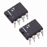
LT1884AIN8 Linear Technology, LT1884AIN8 Datasheet - Page 6

LT1884AIN8
Manufacturer Part Number
LT1884AIN8
Description
IC OPAMP DUAL R-R PICO/IN 8DIP
Manufacturer
Linear Technology
Datasheet
1.LT1884CS8PBF.pdf
(12 pages)
Specifications of LT1884AIN8
Amplifier Type
General Purpose
Number Of Circuits
2
Output Type
Rail-to-Rail
Slew Rate
1 V/µs
Gain Bandwidth Product
2.2MHz
Current - Input Bias
150pA
Voltage - Input Offset
25µV
Current - Supply
850µA
Current - Output / Channel
50mA
Voltage - Supply, Single/dual (±)
2.7 V ~ 36 V, ±1.35 V ~ 18 V
Operating Temperature
-40°C ~ 85°C
Mounting Type
Through Hole
Package / Case
8-DIP (0.300", 7.62mm)
Lead Free Status / RoHS Status
Contains lead / RoHS non-compliant
-3db Bandwidth
-
Available stocks
Company
Part Number
Manufacturer
Quantity
Price
Part Number:
LT1884AIN8#PBF
Manufacturer:
LINEAR/凌特
Quantity:
20 000
LT1884/LT1885
Note 1: Absolute Maximum Ratings are those values beyond which the life
of the device may be impaired.
Note 2: The inputs are protected by back-to-back diodes. If the differential
input voltage exceeds 0.7V, the input current should be limited to less than
10mA.
Note 3: A heat sink may be required to keep the junction temperature
below absolute maximum.
Note 4: The LT1884C/LT1885C and LT1884I/LT1885I are guaranteed
functional over the operating temperature range of – 40 C to 85 C.
Note 5: The LT1884C/LT1885C are designed, characterized and expected
to meet specified performance from – 40 C to 85 C but are not tested or
QA sampled at these temperatures. LT1884I is guaranteed to meet
specified performance from – 40 C to 85 C.
TYPICAL PERFOR A CE CHARACTERISTICS
ELECTRICAL CHARACTERISTICS
6
500
400
300
200
100
24
20
16
12
0
10 A
8
4
0
–0.9 –0.7 –0.5 –0.3 –0.1 0.1 0.3 0.5 0.7 0.9
Distribution of Offset Voltage Drift
V
V
V
OUT
S
S
= 15V
= 15V
vs I
OFFSET VOLTAGE DRIFT ( V/ C)
100 A
SOURCE
I
SOURCE
1mA
25 C
125 C
W
–55 C
10mA
18845 G04
18845 G01
U
140
120
100
–20
–100
–150
–200
80
60
40
20
–50
200
150
100
0
50
0.1
0
Gain vs Frequency
–50 –30 –10 10
Input Offset Voltage
vs Temperature
TEMPCO: –55 C TO 125 C
10 REPRESENTATIVE UNITS
1
10
FREQUENCY (Hz)
TEMPERATURE ( C)
100
1k
30
Note 6: This parameter is not 100% tested.
Note 7: Matching parameters are the difference between amplifiers A and
B in the LT1884 and between amplifiers A and D and B and C in the
LT1885.
Note 8: This parameter is the difference between the two noninverting
input bias currents.
Note 9: CMRR and PSRR are defined as follows: CMRR and PSRR are
measured in V/V on each amplifier. The difference is calculated in V/V
and then converted to dB.
10k 100k 1M 10M
50
70 90 110 125
V
S
= 15V
18845 G05
18845 G02
100
–10
–20
90
80
70
60
50
40
30
20
10
0
10k
Gain, Phase Shift vs Frequency
500
400
300
200
100
0
10 A
V
V
OUT
S
= 15V
100k
vs I
FREQUENCY (Hz)
SINK
PHASE SHIFT
GAIN
100 A
I
SINK
1M
25 C
1mA
125 C
–55 C
18845 G06
10M
18845 G03
–80
–90
–100
–110
–120
–130
–140
–150
–160
–170
–180
10mA


