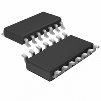
LT1499CS Linear Technology, LT1499CS Datasheet

LT1499CS
Specifications of LT1499CS
Available stocks
Related parts for LT1499CS
LT1499CS Summary of contents
Page 1
... Low Voltage Signal Processing n Battery-Powered Systems L, LT, LTC, LTM, Linear Technology and the Linear logo are registered trademarks and C-Load is a trademark of Linear Technology Corporation. All other trademarks are the property of their respective owners. TYPICAL APPLICATION Single Supply 100kHz 4th Order Butterworth Filter 6 ...
Page 2
... PACKAGE DESCRIPTION LT1498CN8 8-Lead Plastic PDIP 1498 8-Lead Plastic SO LT1498IN8 8-Lead Plastic PDIP 1498I 8-Lead Plastic SO 1498H 8-Lead Plastic SO 1498MP 8-Lead Plastic SO LT1499CS 14-Lead Plastic SO LT1499IS 14-Lead Plastic SO LT1499HS 14-Lead Plastic SO http://www.linear.com/leadfree/ http://www.linear.com/tapeandreel/ TOP VIEW 14 1 OUTA OUT – ...
Page 3
ELECTRICAL CHARACTERISTICS otherwise noted. SYMBOL PARAMETER V Input Offset Voltage OS ΔV Input Offset Voltage Shift OS Input Offset Voltage Match (Channel-to-Channel) I Input Bias Current B ΔI Input Bias Current Shift B Input Bias Current Match (Channel-to-Channel) I Input ...
Page 4
LT1498/LT1499 ELECTRICAL CHARACTERISTICS 0°C < T < 70° 5V, 0V 3V, 0V SYMBOL PARAMETER V Input Offset Voltage Input Offset Voltage Drift (Note 3) OS ΔV Input Offset Voltage ...
Page 5
ELECTRICAL CHARACTERISTICS –40°C < T < 85° 5V, 0V 3V, 0V SYMBOL PARAMETER V Input Offset Voltage Input Offset Voltage Drift (Note 3) OS ΔV Input Offset Voltage Shift ...
Page 6
LT1498/LT1499 ELECTRICAL CHARACTERISTICS –40°C < T < 125° 5V, 0V 3V, 0V SYMBOL PARAMETER V Input Offset Voltage Input Offset Voltage Drift (Note 3) OS ΔV Input Offset Voltage ...
Page 7
ELECTRICAL CHARACTERISTICS –55°C < T < 125° 5V, 0V 3V, 0V SYMBOL PARAMETER V Input Offset Voltage Input Offset Voltage Drift (Note 3) OS ΔV Input Offset Voltage Shift ...
Page 8
LT1498/LT1499 ELECTRICAL CHARACTERISTICS SYMBOL PARAMETER V Input Offset Voltage OS ΔV Input Offset Voltage Shift OS Input Offset Voltage Match (Channel-to-Channel) I Input Bias Current B ΔI Input Bias Current Shift B Input Bias Current Match (Channel-to-Channel) I Input Offset ...
Page 9
ELECTRICAL CHARACTERISTICS 0°C < T < 70° ±15V 0V OUT SYMBOL PARAMETER V Input Offset Voltage Input Offset Voltage Drift (Note 3) OS ΔV Input Offset Voltage Shift OS ...
Page 10
LT1498/LT1499 ELECTRICAL CHARACTERISTICS –40°C < T < 85° ±15V 0V SYMBOL PARAMETER V Input Offset Voltage Input Offset Voltage Drift (Note 3) OS ΔV Input Offset Voltage Shift OS ...
Page 11
ELECTRICAL CHARACTERISTICS –40°C < T < 125° ±15V 0V SYMBOL PARAMETER V Input Offset Voltage Input Offset Voltage Drift (Note 3) OS ΔV Input Offset Voltage Shift OS Input ...
Page 12
LT1498/LT1499 ELECTRICAL CHARACTERISTICS –55°C < T < 125° ±15V 0V SYMBOL PARAMETER V Input Offset Voltage Input Offset Voltage Drift (Note 3) OS ΔV Input Offset Voltage Shift OS ...
Page 13
TYPICAL PERFORMANCE CHARACTERISTICS V Distribution (PNP Stage) 25 LT1498: N8, S8 PACKAGES LT1499: S14 PACKAGE –500 –300 –100 100 300 INPUT ...
Page 14
LT1498/LT1499 TYPICAL PERFORMANCE CHARACTERISTICS Minimum Supply Voltage 300 250 200 150 100 T = 85° 70° NONFUNCTIONAL –55° 25° TOTAL SUPPLY VOLTAGE (V) 14989 ...
Page 15
... NONINVERTING –8 –10 1.5 2.0 2 SETTLING TIME (μs) 14989 G20 Warm-Up Drift vs Time 10 S8 PACKAGE PACKAGE –10 LT1499CS 2. PACKAGE –20 N8 PACKAGE, V –30 LT1499CS, V – 100 TIME AFTER POWER-UP (SEC) 14989 G23 Total Harmonic Distortion + Noise vs Frequency 1. P 10k – ...
Page 16
LT1498/LT1499 TYPICAL PERFORMANCE CHARACTERISTICS 5V Small-Signal Response 200ns/DIV 20mV AT 50kHz IN P ±15V Small-Signal Response V = 15V 200ns/DIV ...
Page 17
APPLICATIONS INFORMATION Rail-to-Rail Input and Output The LT1498/LT1499 are fully functional for an input and output signal range from the negative supply to the posi- tive supply. Figure 1 shows a simplifi ed schematic of the amplifi er. The input ...
Page 18
LT1498/LT1499 APPLICATIONS INFORMATION Overdrive Protection To prevent the output from reversing polarity when the input voltage exceeds the power supplies, two pair of crossing diodes are employed. When the input voltage exceeds either power supply by approximately ...
Page 19
TYPICAL APPLICATIONS Voltage Controlled Current Source 0.5Ω 500pF – 100Ω 1/2 LT1498 – OUT 0.5Ω t < 1μ Voltage Controlled Current Sink + ...
Page 20
LT1498/LT1499 PACKAGE DESCRIPTION .300 – .325 (7.620 – 8.255) .008 – .015 (0.203 – 0.381) +.035 .325 –.015 +0.889 8.255 –0.381 NOTE: 1. DIMENSIONS ARE MILLIMETERS *THESE DIMENSIONS DO NOT INCLUDE MOLD FLASH OR PROTRUSIONS. MOLD FLASH OR PROTRUSIONS SHALL ...
Page 21
PACKAGE DESCRIPTION .050 BSC .245 MIN .030 .005 TYP RECOMMENDED SOLDER PAD LAYOUT .010 – .020 (0.254 – 0.508) .008 – .010 (0.203 – 0.254) (0.406 – 1.270) NOTE: 1. DIMENSIONS IN (MILLIMETERS) 2. DRAWING NOT TO SCALE 3. THESE ...
Page 22
LT1498/LT1499 PACKAGE DESCRIPTION .050 BSC N .245 MIN .030 .005 TYP RECOMMENDED SOLDER PAD LAYOUT .010 – .020 45 (0.254 – 0.508) .008 – .010 (0.203 – 0.254) .016 – .050 (0.406 – 1.270) NOTE: INCHES 1. ...
Page 23
... Updated Conditions for A VOL Information furnished by Linear Technology Corporation is believed to be accurate and reliable. However, no responsibility is assumed for its use. Linear Technology Corporation makes no representa- tion that the interconnection of its circuits as described herein will not infringe on existing patent rights. in Electrical Characteristics Section ...
Page 24
... Drift, 1MHz GBW, 1V/μs OS(MAX) , 6μV/°C Max OS(MAX) , 6μV/°C Max OS(MAX) , Max Supply OS(MAX) , 400kHz GBW, 0.13V/μs Slew Rate, Max Supply – Independent of V < 50μV, I < 400pA 0410 REV G • PRINTED IN USA © LINEAR TECHNOLOGY CORPORATION 2009 . This A + 14989fg ...


