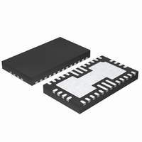
LT6604CUFF-2.5#PBF Linear Technology, LT6604CUFF-2.5#PBF Datasheet - Page 8

LT6604CUFF-2.5#PBF
Manufacturer Part Number
LT6604CUFF-2.5#PBF
Description
IC AMP DIFF LN DUAL 34-QFN
Manufacturer
Linear Technology
Datasheet
1.LT6604IUFF-2.5PBF.pdf
(16 pages)
Specifications of LT6604CUFF-2.5#PBF
Amplifier Type
Differential
Number Of Circuits
2
Output Type
Differential
Current - Input Bias
15µA
Voltage - Input Offset
5000µV
Current - Supply
28mA
Voltage - Supply, Single/dual (±)
3 V ~ 11 V, ±1.5 V ~ 5.5 V
Operating Temperature
0°C ~ 70°C
Mounting Type
Surface Mount
Package / Case
34-QFN
No. Of Amplifiers
2
Input Offset Voltage
35mV
Bandwidth
2.5MHz
Supply Voltage Range
3V To 11V
Supply Current
28mA
Amplifier Case Style
QFN
No. Of Pins
34
Rohs Compliant
Yes
Lead Free Status / RoHS Status
Lead free / RoHS Compliant
Current - Output / Channel
-
-3db Bandwidth
-
Slew Rate
-
Gain Bandwidth Product
-
Available stocks
Company
Part Number
Manufacturer
Quantity
Price
LT6604-2.5
+OUTA, – OUTA (Pins 27, 29): Output Pins. Pins 27 and
29 are the fi lter differential outputs for channel A. With a
typical short-circuit current greater than ±40mA, each pin
can drive a 100Ω and/or 50pF load to AC ground.
V
supply, see Block Diagram. For single supply operation
the V
ceramic capacitor to V
34 can be bypassed or connected to a high quality DC
BLOCK DIAGRAM
PIN FUNCTIONS
8
MIDA
MIDA
(Pin 34): The V
pin should be bypassed with a quality 0.01μF
V
V
V
V
IN
IN
IN
IN
MIDA
+
–
+
–
–
A
B
A
B
. For dual supply operation, Pin
R
R
R
R
V
V
pin is internally biased at mid-
IN
IN
OCMA
IN
IN
MIDB
+INA
–INA
+INB
–INB
NC
NC
NC
NC
NC
NC
V
–
+
+
V
–
V
–
1580Ω
1580Ω
1580Ω
1580Ω
OCM
OCM
OP AMP
OP AMP
–
–
+
+
V
V
MIDA
OCMB
NC
NC
ground. A ground plane should be used. A poor ground
will increase noise and distortion. Pin 34 sets the output
common mode voltage of the 1st stage of the fi lter in chan-
nel A. It has a 5.5kΩ impedance, and it can be overridden
with an external low impedance voltage source.
Exposed Pad (Pin 35): V
soldered to the PCB. If V
the Exposed Pad to V
V
V
800Ω
800Ω
800Ω
800Ω
V
V
+
+
–
–
A
B
11k
11k
11k
11k
NC
V
–
+ –
V
+ –
V
–
–
V
V
800Ω
800Ω
800Ω
800Ω
OCM
OCM
+
–
B
FILTER STAGE
FILTER STAGE
+
+
LOWPASS
LOWPASS
–
.
–
660025 BD
–
. The Exposed Pad must be
is separate from ground, tie
NC
–OUTA
NC
+OUTA
NC
V
V
NC
NC
–OUTB
NC
+OUTB
NC
+
–
A
660425fa


