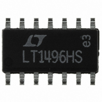
LT1496HS#PBF Linear Technology, LT1496HS#PBF Datasheet - Page 11

LT1496HS#PBF
Manufacturer Part Number
LT1496HS#PBF
Description
IC OP-AMP R-R IN/OUT QUAD 14SOIC
Manufacturer
Linear Technology
Series
Over-The-Top®r
Datasheet
1.LT1494CS8PBF.pdf
(16 pages)
Specifications of LT1496HS#PBF
Amplifier Type
General Purpose
Number Of Circuits
4
Output Type
Rail-to-Rail
Slew Rate
0.001 V/µs
Gain Bandwidth Product
2.7kHz
Current - Input Bias
25pA
Voltage - Input Offset
200µV
Current - Supply
1.4µA
Current - Output / Channel
1.5mA
Voltage - Supply, Single/dual (±)
2.2 V ~ 36 V, ±1.1 V ~ 18 V
Operating Temperature
-40°C ~ 125°C
Mounting Type
Surface Mount
Package / Case
14-SOIC (3.9mm Width), 14-SOL
Lead Free Status / RoHS Status
Lead free / RoHS Compliant
-3db Bandwidth
-
Available stocks
Company
Part Number
Manufacturer
Quantity
Price
APPLICATIONS
The input stage is formed by two diff amps Q1-Q2 and Q3-
Q6. For signals with a common mode voltage between V
and (V
common mode exceeds (V
diverting the current from diff amp Q1-Q2 to current
mirror Q8-Q9. The current from Q8 biases on the other diff
amp consisting of PNP’s Q5-Q6 and NPN’s Q3-Q4. Though
Q5-Q6 are driven from the emitters rather than the base,
the basic diff amp action is the same. When the common
mode voltage is between (V
and Q4 act as followers, forming a buffer between the
amplifier inputs and the emitters of the Q5-Q6. If the
common mode voltage is taken above V
diodes D1 and D2 reverse bias and devices Q3 and Q4 then
CC
IN
IN
+
–
– 0.8V), Q1 and Q2 are active. When the input
Q1
Q10
U
Q2
INFORMATION
0.5
0.5
U
Q5
CC
Q3
CC
– 0.8V) and V
D1
Q9
– 0.8V), Q7 turns on,
Q4
W
Q6
0.5
0.5
D2
Q7
Q8
CC
CC
, devices Q3
Figure 3. Simplified Schematic
(V
, Schottky
V +
U
+
) – 0.8V
EE
Q16
D3
act as diodes. The diff amp formed by Q5-Q6 operates
normally, however, the input bias current increases to the
emitter current of Q5-Q6, which is typically 180nA. The
graph, Input Bias Current vs Common Mode Voltage
found in the Typical Performance Characteristics section,
shows these transitions at three temperatures.
The collector currents of the two-input pairs are combined
in the second stage consisting of Q11 to Q16, which
furnishes most of the voltage gain. Capacitor C1 sets the
amplifier bandwidth. The output stage is configured for
maximum swing by the use of common emitter output
devices Q21 and Q22. Diodes D4 to D6 and current source
Q15 set the output quiescent current.
Q11
Q13
R1
Q12
Q14
R2
Q17
+
I
2
C1
LT1494/LT1495/LT1496
+
Q15
D4
D5
D6
+
D7
I
1
Q19
Q20
Q18
Q21
Q22
1495 F03
OUT
11


