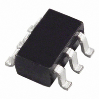
ADA4841-1YRJZ-R2 Analog Devices Inc, ADA4841-1YRJZ-R2 Datasheet - Page 14

ADA4841-1YRJZ-R2
Manufacturer Part Number
ADA4841-1YRJZ-R2
Description
IC OPAMP VF R-R LP LN SOT23-6
Manufacturer
Analog Devices Inc
Datasheet
1.ADA4841-1YRZ-R7.pdf
(20 pages)
Specifications of ADA4841-1YRJZ-R2
Slew Rate
13 V/µs
Amplifier Type
Voltage Feedback
Number Of Circuits
1
Output Type
Rail-to-Rail
-3db Bandwidth
80MHz
Current - Input Bias
3µA
Voltage - Input Offset
40µV
Current - Supply
1.5mA
Current - Output / Channel
60mA
Voltage - Supply, Single/dual (±)
2.7 V ~ 12 V, ±1.35 V ~ 6 V
Operating Temperature
-40°C ~ 125°C
Mounting Type
Surface Mount
Package / Case
SOT-23-6
Op Amp Type
Low Power
No. Of Amplifiers
1
Bandwidth
80MHz
Supply Voltage Range
2.7V To 12V
Amplifier Case Style
SOT-23
No. Of Pins
6
Lead Free Status / RoHS Status
Lead free / RoHS Compliant
Gain Bandwidth Product
-
Lead Free Status / RoHS Status
Lead free / RoHS Compliant, Lead free / RoHS Compliant
ADA4841-1/ADA4841-2
The output noise spectral density can be calculated by
where:
k is Boltzmann’s Constant.
T is the absolute temperature, degrees Kelvin.
ien is the amplifier input current noise spectral density, pA/√Hz.
ven is the amplifier input voltage spectral density, nV/√Hz.
R
R
Figure 40.
Source resistance noise, amplifier voltage noise ( ven ), and the
voltage noise from the amplifier current noise ( ien × R
all subject to the noise gain term (1 + R
2.1 nV/√Hz input voltage noise and 1.4 pA/√Hz input current,
the noise contributions of the amplifier are relatively small for
source resistances between approximately 200 Ω and 30 kΩ.
Figure 41
source resistance. In addition, the value of the feedback resistors
used impacts the noise. It is recommended to keep the value of
feedback resistors between 250 Ω and 1 kΩ to keep the total
noise low.
HEADROOM CONSIDERATIONS
The ADA4841-1/ADA4841-2 are designed to provide maximum
input and output signal ranges with 16-bit to 18-bit dc linearity.
As the input or output headroom limits are reached, the signal
linearity degrades.
vout
S
F
4
is the source resistance as shown in Figure 40.
and R
kTRf
1000
_
100
0.1
en
10
1
10
+
G
=
shows the total RTI noise due to the amplifier vs. the
⎛
⎜
⎜
⎝
are the feedback network resistances, as shown in
1
+
SOURCE RESISTANCE NOISE
R
R
Figure 41. RTI Noise vs. Source Resistance
G
F
⎞
⎟
⎟
⎠
2
[
4
100
kTRs
SOURCE RESISTANCE (Ω)
AMPLIFIER + RESISTOR NOISE
+
ien
2
R
S
1k
2
+
ven
TOTAL AMPLIFIER NOISE
F
2
/R
]
+
G
⎛
⎜
⎜
⎝
). Note that with a
R
R
10k
G
F
⎞
⎟
⎟
⎠
2
4
kTRg
S
) are
+
100k
ien
Rev. E | Page 14 of 20
(6)
2
R
F
2
The input stage positive limit is almost exactly a volt below the
positive supply at room temperature. Input voltages above that
start to show clipping behavior. The positive input voltage limit
increases with temperature with a coefficient of about 2 mV/°C.
The lower supply limit is nominally below the minus supply;
therefore, in a standard gain configuration, the output stage
limits the signal headroom on the negative supply side. Figure 42
and Figure 43 show the nominal CMRR behavior at the limits of
the input headroom for three temperatures—this is generated
using the subtractor topology shown in Figure 44, which avoids
the output stage limitation.
–100
–140
–180
–220
–260
–300
300
260
220
180
140
100
–20
–60
60
20
–100
–150
–200
–250
–300
–350
–400
–450
–500
–550
–600
–650
–700
–750
–800
–50
3.00
–6.00
0
+125°C
–40°C
+25°C
3.20
Figure 42. +CMV vs. Common-Mode Error vs. V
–5.80 –5.60 –5.40 –5.20 –5.00 –4.80 –4.60 –4.40 –4.20
Figure 43. −CMV vs. Common-Mode Error vs. V
– V
CM
Figure 44. Common-Range Subtractor
3.40
+
COMMON-MODE VOLTAGE (V)
3.60
COMMON-MODE VOLTAGE (V)
3.80
4.00
4.20
+ V
4.40
OUT
–
4.60
OS
OS
+125°C
–40°C
+25°C
4.80
–4.00
5.00


