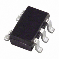
AD8065ARTZ-R2 Analog Devices Inc, AD8065ARTZ-R2 Datasheet - Page 14

AD8065ARTZ-R2
Manufacturer Part Number
AD8065ARTZ-R2
Description
IC OPAMP VF R-R LN LP SOT23-5
Manufacturer
Analog Devices Inc
Series
FastFET™r
Datasheet
1.AD8065ARTZ-REEL7.pdf
(28 pages)
Specifications of AD8065ARTZ-R2
Slew Rate
180 V/µs
Design Resources
Unipolar, Precision DC Digital-to-Analog Conversion Using AD5426/32/43 8-Bit to12-Bit DACs (CN0034) Programmable Gain Element Using AD5426/32/43 Current Output DACs (CN0038) Programmable Gain Element Using AD5450/1/2/3 Current Output DAC Family (CN0055)
Amplifier Type
Voltage Feedback
Number Of Circuits
1
Output Type
Rail-to-Rail
-3db Bandwidth
145MHz
Current - Input Bias
3pA
Voltage - Input Offset
400µV
Current - Supply
6.6mA
Current - Output / Channel
30mA
Voltage - Supply, Single/dual (±)
5 V ~ 24 V, ±2.5 V ~ 12 V
Operating Temperature
-40°C ~ 85°C
Mounting Type
Surface Mount
Package / Case
SOT-23-5, SC-74A, SOT-25
Op Amp Type
Voltage Feedback
No. Of Amplifiers
1
Bandwidth
145MHz
Supply Voltage Range
5V To 24V
Amplifier Case Style
SOT-23
No. Of Pins
5
Lead Free Status / RoHS Status
Lead free / RoHS Compliant
Gain Bandwidth Product
-
Lead Free Status / RoHS Status
Lead free / RoHS Compliant, Lead free / RoHS Compliant
Available stocks
Company
Part Number
Manufacturer
Quantity
Price
Part Number:
AD8065ARTZ-R2
Manufacturer:
ADI/亚德诺
Quantity:
20 000
AD8065/AD8066
+0.1%
–0.1%
–0.1
–0.2
–0.3
–10
–15
–20
–25
–30
0.3
0.2
0.1
–5
0
0
–14
25
Figure 30. Input Offset Voltage vs. Common-Mode Voltage
–12
Figure 28. Long-Term Settling Time (See Figure 49)
Figure 29. Input Bias Current vs. Temperature
–10
35
t = 0
2mV/DIV
–8 –6 –4
V
S
COMMON-MODE VOLTAGE (V)
= ±5V
45
TEMPERATURE (°C)
V
–2
S
= +5V
55
0
V
V
IN
OUT
2
= 140mV/DIV
– 2V
4
65
IN
+I
–I
6
b
64 μ s/DIV
b
8
75
V
S
10 12 14
= ±12V
85
Rev. J | Page 14 of 28
+0.1%
–0.1%
–10
–15
–20
–25
–30
42
40
35
30
25
20
15
10
36
30
24
18
12
10
–5
Figure 32. Input Bias Current vs. Common-Mode Voltage Range
6
0
5
0
5
0
–2.0
–12
Figure 31. 0.1% Short-Term Settling Time (See Figure 49)
(See the Input and Output Overload Behavior Section)
–10
–I b
2mV/DIV
–1.5
–8
–1.0
t = 0
+I b
–6
Figure 33. Input Offset Voltage
INPUT OFFSET VOLTAGE (mV)
COMMON-MODE VOLTAGE (V)
–4
–0.5
–2
0
0
2
0.5
V
IN
4
= 500mV/DIV
–I b
N = 299
SD = 0.388
MEAN = –0.069
1.0
6
+I b
V
OUT
10ns/DIV
8
1.5
– 2V
10
IN
2.0
12


