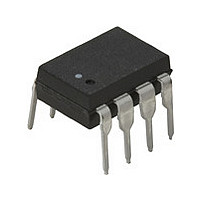
HCPL-7520 Avago Technologies US Inc., HCPL-7520 Datasheet - Page 8

HCPL-7520
Manufacturer Part Number
HCPL-7520
Description
OPTOCOUPLER AMP 100KHZ 8-DIP
Manufacturer
Avago Technologies US Inc.
Datasheet
1.HCPL-7520-000E.pdf
(16 pages)
Specifications of HCPL-7520
Amplifier Type
Isolation
Number Of Circuits
1
-3db Bandwidth
100kHz
Current - Input Bias
600nA
Voltage - Input Offset
600µV
Current - Supply
11.7mA
Current - Output / Channel
16mA
Voltage - Supply, Single/dual (±)
4.5 V ~ 5.5 V
Operating Temperature
-40°C ~ 85°C
Mounting Type
Through Hole
Package / Case
8-DIP (0.300", 7.62mm)
Operating Supply Voltage (typ)
5V
Lead Free Status / RoHS Status
Contains lead / RoHS non-compliant
Output Type
-
Slew Rate
-
Gain Bandwidth Product
-
Lead Free Status / RoHS Status
Not Compliant, Contains lead / RoHS non-compliant
Available stocks
Company
Part Number
Manufacturer
Quantity
Price
Company:
Part Number:
HCPL-7520
Manufacturer:
MAXIM
Quantity:
223
Company:
Part Number:
HCPL-7520-000E
Manufacturer:
AVAGO
Quantity:
7 000
Company:
Part Number:
HCPL-7520-060
Manufacturer:
AVAGO
Quantity:
1 400
Company:
Part Number:
HCPL-7520-060E
Manufacturer:
AVAGO
Quantity:
1 400
Company:
Part Number:
HCPL-7520-300
Manufacturer:
AVAGO
Quantity:
1 400
Part Number:
HCPL-7520-300E
Manufacturer:
AVAGO/安华高
Quantity:
20 000
Part Number:
HCPL-7520V-000E
Manufacturer:
AVAGO/安华高
Quantity:
20 000
Part Number:
HCPL-7520V-500E
Manufacturer:
AVAGO/安华高
Quantity:
20 000
Switching Specifications (AC)
Over recommended operating conditions unless otherwise specified.
Parameter
V
V
V
V
V
V
V
Common Mode Transient
Immunity
Package Characteristics
Parameter
Input-Output Momentary
Withstand Voltage
Input-Output Resistance
Input-Output Capacitance
Notes:
General Note: Typical values were taken from a sample of nominal units operating at nominal conditions (V
1. Input Offset Voltage is defined as the DC Input Voltage required to obtain an output voltage of V
2. Gain is defined as the slope of the best-fit line of the output voltage vs. the differential input voltage (V
3. Nonlinearity is defined as half of the peak-to-peak output deviation from the best-fit gain line, expressed as a percentage of the full-scale output
4. NL
5. NL
6. In accordance with UL1577, each optocoupler is proof tested by applying an insulation test voltage ≥ 4500 Vrms for 1 second (leakage
7. CMRR is defined as the ratio of the differential signal gain (signal applied differentially between pins 2 and 3) to the common-mode gain (input
8
IN
IN
IN
OUT
OUT
OUT
OUT
= 25°C) unless otherwise stated. Nominal plots shown from Figure 1 to 11 represented the drift of these nominal units from their nominal
operating conditions.
Gain is derived from V
voltage range.
detection current limit, I
IEC/EN/DIN EN 60747-5-2 Insulation Characteristic Table, if applicable.
pins tied together and the signal applied to both inputs at the same time), expressed in dB.
to V
to V
to V
200
100
Rise Time (10 – 90%)
Fall Time (10 – 90%)
Bandwidth (-3 dB)
Noise
is the nonlinearity specified over an input voltage range of ±200 mV.
is the nonlinearity specified over an input voltage range of ±100 mV.
OUT
OUT
OUT
Signal Delay (50 – 10%) t
Signal Delay (50 – 50%) t
Signal Delay (50 – 90%) t
REF
/512 mV; e.g. V
I-O
≤ 5 µA). This test is performed before the 100% production test for the partial discharge (method b) shown in
Symbol
V
R
C
I-O
ISO
I-O
REF
Symbol Min. Typ.
t
t
BW
N
CMTI
PD10
PD50
PD90
R
F
= 5.0, gain will be 9.77 V/V.
OUT
Min.
3750
50
10
Typ.
>10
1.4
2.2
3.4
5.2
3.0
3.2
100
31.5
15
9
Max.
4
5
9.9
7
7
Max.
Units
µs
µs
µs
µs
µs
kHz
mVrms V
kV/µs
Units
V
Ω
pF
rms
Test Conditions
V
V
V
V
V
T
A
IN+
IN+
IN+
IN+
IN+
IN+
REF
= 25°C, V
Test Conditions
T
V
Freq = 1 MHz
A
= 0 mV to 200 mV step 13
= 0 mV to 200 mV step 13
= 0 mV to 200 mV step 13
= 0 mV to 200 mV step 13
= 200 mV
= 0 V
/2.
I-O
= 25°C, RH < 50%
DD1
IN+
= 500 V
= V
- V
CM
IN-
DD2
) over the specified input range.
pk-pk
= 1000 V
= 5 V, V
REF
= 4.0 V, Temperature
Fig.
Fig. Note
14
15
Note
6


