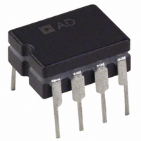
AD844BQ Analog Devices Inc, AD844BQ Datasheet - Page 16

AD844BQ
Manufacturer Part Number
AD844BQ
Description
IC OPAMP CF 60MHZ 80MA 8CDIP
Manufacturer
Analog Devices Inc
Datasheet
1.AD844ANZ.pdf
(20 pages)
Specifications of AD844BQ
Slew Rate
2000 V/µs
Rohs Status
RoHS non-compliant
Amplifier Type
Current Feedback
Number Of Circuits
1
-3db Bandwidth
60MHz
Current - Input Bias
150pA
Voltage - Input Offset
50µV
Current - Supply
6.5mA
Current - Output / Channel
80mA
Voltage - Supply, Single/dual (±)
±4.5 V ~ 18 V
Operating Temperature
-40°C ~ 85°C
Mounting Type
Through Hole
Package / Case
8-CDIP (0.300", 7.62mm)
Op Amp Type
High Speed
No. Of Amplifiers
1
Bandwidth
60MHz
Supply Voltage Range
± 4.5V To ± 18V
Amplifier Case Style
DIP
No. Of Pins
8
Output Type
-
Gain Bandwidth Product
-
Lead Free Status / RoHS Status
Contains lead / RoHS non-compliant
Available stocks
Company
Part Number
Manufacturer
Quantity
Price
AD844
DC ERROR CALCULATION
Figure 37 shows a model of the dc error and noise sources for
the AD844. The inverting input bias current, I
feedback resistor. I
in the resistance at Pin 3 (R
any offset voltage) appears at the inverting input. The total
error, V
Because I
inserting a resistor in series with the noninverting input does
not necessarily reduce dc error and may actually increase it.
NOISE
Noise sources can be modeled in a manner similar to the dc bias
currents, but the noise sources are I
induced noise at the output, V
Overall noise can be reduced by keeping all resistor values to a
minimum. With typical numbers, R1 = R2 = 1 kΩ, R
V
calculates to 12 nV/√Hz. The current noise is dominant in this
case, because it is in most low gain applications.
VIDEO CABLE DRIVER USING ±5 V SUPPLIES
The AD844 can be used to drive low impedance cables. Using
±5 V supplies, a 100 Ω load can be driven to ±2.5 V with low
distortion. Figure 38 shows an illustrative application that
provides a noninverting gain of +2, allowing the cable to be
reverse-terminated while delivering an overall gain of +1 to the
load. The −3 dB bandwidth of this circuit is typically 30 MHz.
Figure 39 shows a differential gain and phase test setup. In video
applications, differential-phase and differential-gain characteris-
tics are often important. Figure 40 shows the variation in phase as
the load voltage varies. Figure 41 shows the gain variation.
N
R2
= 2 nV/√Hz, I
V
V
O
ON
O
Figure 37. Offset Voltage and Noise Model for the AD844
=
, at the output is:
BN
=
(
V
I
N
and I
BP
(
(
R
I
P
NP
R
BP
NP
P
+
I
I
NN
BP
NP
R
are unrelated both in sign and magnitude,
V
= 10 pA/√Hz, I
, the noninverting input bias current, flows
P
OS
)
2
+
+
V
I
P
BN
N
), and the resulting voltage (plus
AD844
2
R
ON
I
I
BN
BP
)
R
⎛ +
⎜
⎝
IN
IN
, is:
1
)
⎛ +
⎜
⎝
NN
1
NN
R2
R1
, I
= 12 pA/√Hz, and V
⎞
⎟
⎠
R1
R2
V
NP
2
OS
R1
, V
+
⎞
⎟
⎠
(
+
I
N
, and the amplifier
NN
I
BN
BN
, flows in the
R1
R1
)
2
P
= 0 Ω,
ON
Rev. F | Page 16 of 20
GENERATOR
STAIRCASE
ANALYZER
NETWORK
HP3314A
HP8753A
–0.02
–0.04
–0.06
0.06
0.04
0.02
–0.1
–0.2
–0.3
V
0.3
0.2
0.1
EXT
TRIG
SYNC OUT
0
IN
0
50Ω
0
Figure 40. Differential Phase for the Circuit of Figure 38
0
Figure 41. Differential Gain for the Circuit of Figure 38
IRE = 7.14mV
IRE = 7.14mV
RF OUT
RF IN
OUT
Figure 39. Differential Gain/Phase Test Setup
Figure 38. The AD844 as a Cable Driver
3
2
18
18
(TERMINATOR)
+5V
–5V
4
OUT
7
6
IN
2.2µF
2.2µF
36
36
50Ω
HP11850C
SPLITTER
V
V
OUT
OUT
300Ω
300Ω
(IRE)
(IRE)
OUT
50Ω
54
54
Z
OUT
O
= 50Ω
V
V
IN
IN
470Ω
72
72
R
50Ω
CIRCUIT
UNDER
L
TEST
V
OUT
V
90
9
OUT
0


