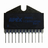
PA93 Cirrus Logic Inc, PA93 Datasheet - Page 5

PA93
Manufacturer Part Number
PA93
Description
IC PWR AMP 400V 8A 12SIP
Manufacturer
Cirrus Logic Inc
Series
Apex Precision Power™r
Specifications of PA93
Amplifier Type
Power
Number Of Circuits
1
Slew Rate
50 V/µs
Gain Bandwidth Product
12MHz
Current - Input Bias
200pA
Voltage - Input Offset
2000µV
Current - Supply
10mA
Current - Output / Channel
8A
Voltage - Supply, Single/dual (±)
80 V ~ 400 V, ±40 V ~ 200 V
Operating Temperature
-25°C ~ 85°C
Mounting Type
Through Hole
Package / Case
12-SIP
Number Of Channels
1
Voltage Gain Db
111 dB
Common Mode Rejection Ratio (min)
80 dB
Input Offset Voltage
10 mV
Maximum Operating Temperature
+ 85 C
Mounting Style
Through Hole
Maximum Dual Supply Voltage
+/- 200 V
Minimum Operating Temperature
- 25 C
For Use With
598-1390 - KIT EVAL PA90,91,92,93,98 PINOUT
Lead Free Status / RoHS Status
Contains lead / RoHS non-compliant
Output Type
-
-3db Bandwidth
-
Lead Free Status / Rohs Status
In Transition
Other names
598-1333
Available stocks
Company
Part Number
Manufacturer
Quantity
Price
SAFE OPERATING AREA (SOA)
The MOSFET output stage of this power operational am-
plifier has two distinct limitations:
1. The current handling capability of the MOSFET geom-
2. The junction temperature of the output MOSFETs.
NOTE: The output stage is protected against transient
flyback. However, for protection against sustained, high
energy flyback, external fast-recovery diodes should be
used.
SAFE OPERATING CURVES
The safe operating area curves define the maximum ad-
ditional internal power dissipation the amplifier can toler-
ate when it produces the necessary output to drive an
external load.
INPUT PROTECTION
Although the PA93 can withstand differential voltages up
to ±20V, additional external protection is recommended.
Low leakage, low capacitance JFETs connected as di-
odes are recommended (e.g. 2N4416, Q1-Q4 in Figure 2). The differen-
tial input voltage will be clamped to ±1.4V. This is sufficient overdrive to
produce maximum power bandwidth.
POWER SUPPLY PROTECTION
Unidirectional zener diode transient suppressors are recommended as
protection on the supply pins. See Figure 2. The zeners clamp transients
to voltages within the power supply rating and also clamp power supply
reversals to ground. Whether the zeners are used or not, the system
power supply should be evaluated for transient performance including
power-on overshoot and power-off polarity reversals as well as line regu-
lation.
Conditions which can cause open circuits or polarity reversals on either
power supply rail should be avoided or protected against. Reversals or opens on the negative supply rail is known
to induce input stage failure. Unidirectional transzorbs prevent this, and it is desirable that they be both electrically
and physically as close to the amplifier as possible.
STABILITY
The PA93 is externally compensated and performance can be tailored to the application. Use the graphs of small
signal response and power response as a guide. The compensation capacitor C
voltage. An NPO capacitor is recommended. The compensation network C
plifier pins 4 and 5 to avoid spurious oscillation.
QUIESCENT CURRENT REDUCTION
When pin 3 (I
but also raises distortion since the output stage is then class C biased. The output stage bias current is nominally
set at 1mA. Pin 3 may be left open if not used.
PA93U
etry and the wire bonds.
Q
) is shorted to pin 5 (CC2) the AB biasing of the output stage is disabled. This lowers quiescent power
P r o d u c t T e c h n o l o g y F r o m
.08
.06
20
10
.8
.6
.4
.3
.2
.1
8
6
4
3
2
1
10
SUPPLY TO OUTPUT DIFFERENTIAL, V
20
DC, T
C
–IN
+IN
FIGURE 2.
OVERVOLTAGE
PROTECTION
R
C
30 40
Q1
must be mounted closely to the am-
C
= 25C
Q2
C
must be rated at 500V working
200mS
60 80
SOA
100
Q4
Q3
2
1
+V
PA93
–V
200
S
11, 12
7, 8
S
Z1
Z2
S
– V
300
O
PA93
(V)
6
500
5


