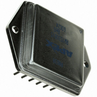
PA03A Cirrus Logic Inc, PA03A Datasheet - Page 4

PA03A
Manufacturer Part Number
PA03A
Description
IC PWR AMP 150V 30A AGRADE 12DIP
Manufacturer
Cirrus Logic Inc
Series
Apex Precision Power™r
Datasheet
1.PA03.pdf
(5 pages)
Specifications of PA03A
Amplifier Type
Power
Number Of Circuits
1
Slew Rate
8 V/µs
Gain Bandwidth Product
1MHz
Current - Input Bias
3pA
Voltage - Input Offset
250µV
Current - Supply
125mA
Current - Output / Channel
30A
Voltage - Supply, Single/dual (±)
30 V ~ 150 V, ±15 V ~ 75 V
Operating Temperature
-25°C ~ 85°C
Mounting Type
Through Hole
Package / Case
12-DIP Module
Lead Free Status / RoHS Status
Contains lead / RoHS non-compliant
Output Type
-
-3db Bandwidth
-
Other names
598-1419
PA03A
PA03A
Available stocks
Company
Part Number
Manufacturer
Quantity
Price
Part Number:
PA03A
Manufacturer:
APEX
Quantity:
20 000
PA03 • PA03A
GENERAL
siderations" which covers stability, supplies, heat sinking,
mounting, current limit, SOA interpretation, and specification
interpretation. Visit www.cirrus.com for design tools that help
automate tasks such as calculations for stability, internal power
dissipation, current limit; heat sink selection; Apex Precision
Power’s complete Application Notes library; Technical Seminar
Workbook; and Evaluation Kits.
MOUNTING PRECAUTIONS
put any stress on the mounting ears of this package. This calls
for caution when pushing the amplifier into certain types of
packaging foam and particularly when inserting the device into
a socket. Insert the amplifier into the socket only by pushing
on the perimeter of the package lid. Pushing the unit into the
socket by applying pressure to the mounting tabs will bend
the base due to the high insertion force required. The base
will then not contact the heatsink evenly resulting in very poor
heat transfer. To remove a unit from a socket, pry the socket
away from the heatsink so that the heatsink will support the
amplifier base evenly. Recommended mounting torque is 8–10
in.-lbs. (.9–1.13 N•m).
SAFE OPERATING AREA (SOA)
worst case power dissipation calculations must assume cur-
rent capability of 46 amps. Application specific circuits should
be checked against the SOA curve when relying upon current
limit for fault protection.
SAFE OPERATING AREA CURVES
less severe, since junction temperature limiting responds within
10ms. Stress levels shown as being safe for more than 10ms
duration will merely cause thermal shutdown.
shutdown is a sign that the internal junction temperatures have
reached approximately 175°C. Thermal shutdown is a short
term safety feature. If the conditions remain that cause thermal
shutdown, the amplifier will oscillate in and out of shutdown,
creating peak high power stresses, destroying useful signals,
and reducing the reliability of the device.
4
EXTERNAL CONNECTIONS
–SHUT DN
+SHUT DN
–OUTPUT
–SUPPLY
CAUTION
Please read Application Note 1 "General Operating Con-
The PA03 copper base is very soft and easily bent. Do not
Due to the internal (non-adjustable) current limit of the PA03,
Second breakdown limitations do apply to the PA03 but are
Under normal operating conditions, activation of the thermal
–INPUT
+INPUT
1
2
3
4
5
6
VIEW
TOP
The internal substrate contains beryllia (BeO).
Do not break the seal. If accidentally broken, do
not crush, machine, or subject to temperatures
in excess of 850°C to avoid generating toxic
fumes.
†
12
11
10
9
8
7
BALANCE CONTROL
BALANCE CONTROL
PHASE COMP.
PHASE COMP.
+SUPPLY
+OUTPUT
Pins 6 & 7 must be
connected together.
If unused, tie Pins
11 & 12 to +SUPPLY.
† IMPORTANT: OBSERVE
MOUNTING PRECAUTIONS.
REVERSE INSERTION
WILL DESTROY UNIT.
P r o d u c t I n n o v a t i o n F r o m
BALANCE CONTROL
to zero. To implement this adjustment install a 100 to 200 ohm
potentiometer between pins 11 and 12 and connect the wiper
arm to the positive supply. Bypass pins 11 and 12 each with
at least a .01µF ceramic capacitor.
pins 11 and 12 to the positive supply.
OUTPUT STAGE SHUTDOWN
ing one of the circuits shown in Figure 1. There are many
applications for this function. One is a load protection based
on power delivered to the load or thermal rise. Another one is
conservation of power when using batteries. The control volt-
age requirements accommodate a wide variety logic drivers.
1. CMOS operating at +5V can drive the control pins di-
2. CMOS operating at greater than 5V supplies need a voltage
3. TTL logic needs a pull up resistor to +5V to provide a swing
PHASE COMPENSATION
is required to insure stability. In addition to the resistive feed-
back network, roll off or integrating capacitors must also be
considered. A frequency of 1 MHz is most appropriate to cal-
culate gain. Operation at gains below 10, without the external
compensation capacitor opens the possibility of oscillations
near output saturation regions when under load, the improper
operation of the thermal shutdown circuit. This can result in
amplifier destruction.
At gains of 10 or more:
1. No external components are required.
2. Typical slew rate will be 8V/µs.
3. Typical phase margin will be 70°.
The voltage offset of the PA03 may be externally adjusted
If the optional adjust provision is not used, connect both
The entire power stage of the PA03 may be disabled us-
At low gain settings an external compensation capacitor
rectly.
divider.
to the fully disabled voltage (3.5V). When not using the
shutdown feature, connect both pins 3 and 4 to common.
40
30
10
5
1
10
SUPPLY TO OUTPUT DIFFERENTIAL V
T
C
= 25°C
20
SOA
dc
CURRENT LIMIT ZONE
50
S
100
–V
O
PA02U
(V)
150


