LMH6553MR/NOPB National Semiconductor, LMH6553MR/NOPB Datasheet - Page 6
LMH6553MR/NOPB
Manufacturer Part Number
LMH6553MR/NOPB
Description
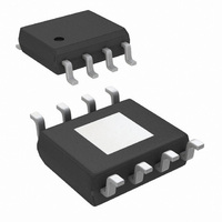
IC AMP DIFF 900MHZ W/CLAMP 8PSOP
Manufacturer
National Semiconductor
Series
LMH®, PowerWise®r
Datasheet
1.LMH6553SDENOPB.pdf
(26 pages)
Specifications of LMH6553MR/NOPB
Amplifier Type
Differential
Number Of Circuits
1
Output Type
Differential
Slew Rate
2300 V/µs
-3db Bandwidth
900MHz
Current - Input Bias
50µA
Current - Supply
29.1mA
Current - Output / Channel
120mA
Voltage - Supply, Single/dual (±)
4.5 V ~ 12 V, ±2.25 V ~ 6 V
Operating Temperature
-40°C ~ 125°C
Mounting Type
Surface Mount
Package / Case
8-PSOP
Lead Free Status / RoHS Status
Lead free / RoHS Compliant
Gain Bandwidth Product
-
Voltage - Input Offset
-
Other names
*LMH6553MR/NOPB
LMH6553MR
LMH6553MR


www.national.com
V
Miscellaneous Performance
Z
PSRR
I
Symbol
S
T
OSCM
Note 1: Absolute Maximum Ratings indicate limits beyond which damage to the device may occur. Operating Ratings indicate conditions for which the device is
intended to be functional, but specific performance is not guaranteed. For guaranteed specifications, see the Electrical Characteristics tables.
Note 2: Electrical Table values apply only for factory testing conditions at the temperature indicated. Factory testing conditions result in very limited self-heating
of the device such that T
T
Individual parameters are tested as noted.
Note 3: The maximum power dissipation is a function of T
P
Note 4: The maximum output current (I
for more details.
Note 5: Human Body Model, applicable std. MIL-STD-883, Method 30157. Machine Model, applicable std. JESD22-A115-A (ESD MM std. of JEDEC). Field-
Induced Charge-Device Model, applicable std. JESD22-C101-C (ESD FICDM std. of JEDEC).
Note 6: Short circuit current should be limited in duration to no more than 10 seconds. See the Power Dissipation section of the Application Information for more
details.
Note 7: Typical values represent the most likely parametric norm as determined at the time of characterization. Actual typical values may vary over time and will
also depend on the application and configuration. The typical values are not tested and are not guaranteed on shipped production material.
Note 8: Limits are 100% production tested at 25°C. Limits over the operating temperature range are guaranteed through correlation using Statistical Quality
Control (SQC) methods.
Note 9: Negative current implies current flowing out of the device.
Note 10: I
Note 11: Exceeding limits could result in excessive device current.
Note 12: Linearity Guardband is defined for an output sinusoid (f = 75 MHz, V
where the SFDR is decreased by 3 dB.
Note 13: Clamp Overshoot Width is the duration of overshoot in a 100% overdrive condition.
Note 14: This parameter is guaranteed by design and/or characterization and is not tested in production. The condition of V
operation; continuous operation with V
J
D
> T
= (T
A
. See Applications Section for information on temperature de-rating of this device." Min/Max ratings are based on product characterization and simulation.
J(MAX)
Output Common Mode Error
Input Bias Current
Voltage Range
CMRR
Input Resistance
Gain
Open Loop Transimpedance
Power Supply Rejection Ratio
Supply Current
BI
is referred to a differential output offset voltage by the following relationship: V
– T
A
) / θ
JA
. All numbers apply for packages soldered directly onto a PC Board.
Parameter
J
= T
A
. No guarantee of parametric performance is indicated in the electrical tables under conditions of internal self-heating where
CLAMP
OUT
) is determined by device power dissipation limitations. See the Power Dissipation section of the Application Section
= 3V may incur permanent damage to the device.
Common Mode, V
V
Measure V
ΔV
Differential
DC, ΔV
R
CM
L
J(MAX)
O,CM
=
= 0,
∞
, θ
/ΔV
S
(Note
JA
= ±1V
. The maximum allowable power dissipation at any ambient temperature is
OD
CM
, V
9)
ID
Conditions
OD
IN
= 0V
6
= 2 V
= float, V
PP
). It is the difference between the V
OD(offset)
CM
= 0
= I
BI
*2R
F
(Note
±0.75
0.995
Min
−20
23
CLAMP
CLAMP
8)
= 3V is not intended for continuous
(Note
level and the peak output voltage
±0.81
−3.5
1.00
26.5
Typ
200
105
84
85
2
7)
(Note
1.008
Max
20
30
34
8)
Units
dBΩ
V/V
mV
mA
kΩ
µA
dB
dB
V
Related parts for LMH6553MR/NOPB
Image
Part Number
Description
Manufacturer
Datasheet
Request
R

Part Number:
Description:
DIFF AMP, 900MHZ, 8PSOP, POWERWISE
Manufacturer:
National Semiconductor
Datasheet:

Part Number:
Description:
National Semiconductor [8-Bit D/A Converter]
Manufacturer:
National Semiconductor
Datasheet:
Part Number:
Description:
National Semiconductor [Media Coprocessor]
Manufacturer:
National Semiconductor
Datasheet:
Part Number:
Description:
Digitally Controlled Tone and Volume Circuit with Stereo Audio Power Amplifier, Microphone Preamp Stage and National 3D Sound
Manufacturer:
National Semiconductor
Datasheet:
Part Number:
Description:
Digitally Controlled Tone and Volume Circuit with Stereo Audio Power Amplifier, Microphone Preamp Stage and National 3D Sound
Manufacturer:
National Semiconductor
Datasheet:
Part Number:
Description:
AC97 Rev 2 Codec with Sample Rate Conversion and National 3D Sound
Manufacturer:
National Semiconductor
Part Number:
Description:
Manufacturer:
National Semiconductor
Datasheet:
Part Number:
Description:
Manufacturer:
National Semiconductor
Datasheet:
Part Number:
Description:
General Purpose, Low Voltage, Low Power, Rail-to-Rail Output Operational Amplifiers
Manufacturer:
National Semiconductor
Datasheet:
Part Number:
Description:
8-bit 20 MSPS flash A/D converter.
Manufacturer:
National Semiconductor
Datasheet:
Part Number:
Description:
Low Noise Quad Operational Amplifier
Manufacturer:
National Semiconductor
Datasheet:
Part Number:
Description:
Quad Differential Line Receivers
Manufacturer:
National Semiconductor
Datasheet:
Part Number:
Description:
Quad High Speed Trapezoidal? Bus Transceiver
Manufacturer:
National Semiconductor
Datasheet:
Part Number:
Description:
Dual Line Receiver
Manufacturer:
National Semiconductor
Datasheet: