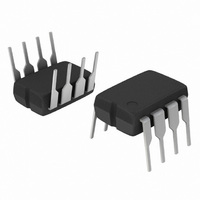
NE5532ANG ON Semiconductor, NE5532ANG Datasheet - Page 5

NE5532ANG
Manufacturer Part Number
NE5532ANG
Description
IC OPAMP DUAL LOW NOISE 8-DIP
Manufacturer
ON Semiconductor
Datasheet
1.NE5532NG.pdf
(10 pages)
Specifications of NE5532ANG
Amplifier Type
General Purpose
Number Of Circuits
2
Slew Rate
9 V/µs
Gain Bandwidth Product
10MHz
Current - Input Bias
200nA
Voltage - Input Offset
500µV
Current - Supply
8mA
Current - Output / Channel
38mA
Voltage - Supply, Single/dual (±)
±3 V ~ 20 V
Operating Temperature
0°C ~ 70°C
Mounting Type
Through Hole
Package / Case
8-DIP (0.300", 7.62mm)
Number Of Channels
2
Common Mode Rejection Ratio (min)
70 dB
Input Voltage Range (max)
Positive Rail - 3 V
Input Voltage Range (min)
Negative Rail + 3 V
Input Offset Voltage
4 mV
Input Bias Current (max)
800 nA
Operating Supply Voltage
+/- 20 V
Supply Current
8 mA
Maximum Power Dissipation
1200 mW
Maximum Operating Temperature
+ 70 C
Minimum Operating Temperature
0 C
Dual Supply Voltage
+/- 5 V, +/- 9 V, +/- 12 V
Maximum Dual Supply Voltage
+/- 20 V
Minimum Dual Supply Voltage
+/- 3 V
Mounting Style
Through Hole
Shutdown
No
Technology
Bipolar
Voltage Gain Db
100 dB
Lead Free Status / RoHS Status
Lead free / RoHS Compliant
Output Type
-
-3db Bandwidth
-
Lead Free Status / Rohs Status
Lead free / RoHS Compliant
Other names
NE5532ANG
NE5532ANGOS
NE5532ANGOS
Available stocks
Company
Part Number
Manufacturer
Quantity
Price
Company:
Part Number:
NE5532ANG
Manufacturer:
ON Semiconductor
Quantity:
1 812
Company:
Part Number:
NE5532ANG
Manufacturer:
ON Semiconductor
Quantity:
5
Part Number:
NE5532ANG
Manufacturer:
ON/安森美
Quantity:
20 000
(mA)
I
O
120
-40
80
40
Figure 2. Open-Loop Frequency
0
80
60
40
20
Figure 5. Output Short−Circuit
0
10
-55
-25
10
2
0
10
Response
3
Current
T
25
amb
f (Hz)
10
I
I
(mA)
P
N
TYPICAL VALUES
4
50
(
o
C)
TYP
10
V
6
4
2
0
5
S
75
= "15 V
0
10
Figure 8. Supply Current
100 +125
6
TYPICAL PERFORMANCE CHARACTERISTICS
10
7
Vp; −V
(mA)
-20
I
10
60
40
20
I
Figure 3. Closed-Loop Frequency
0
10
N
TYP
(V)
3
1,4
1,2
0,8
0,4
RF = 10 kW; RE = 100 W
RF = 9 kW; RE = 1 kW
RF = 1 kW; RE = ∞
0
-55
Figure 6. Input Bias Current
10
http://onsemi.com
4
I
-25
O
= 0
Response
20
10
0
5
f (Hz)
5
T
(nV
25
amb
10
TYPICAL VALUES
Hz )
50
(
6
o
C)
10
10
10
V
−2
−1
−2
10
S
75
1
= "15 V
10
10
Figure 9. Input Noise Voltage
7
100 +125
10
8
10
Vo(p-p)
2
V
Density
(V)
IN
f (Hz)
(V)
TYP
30
20
10
Figure 4. Large−Signal Frequency
0
Figure 7. Input Common−Mode
0
40
30
20
10
0
10
10
2
3
10
Voltage Range
3
Response
Vp; −V
10
10
4
TYPICAL VALUES
10
4
f (Hz)
N
TYPICAL VALUES
(V)
10
V
5
S
= "15 V
10
6
20
10
7


