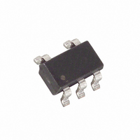
MAX4012EUK+T Maxim Integrated Products, MAX4012EUK+T Datasheet - Page 11

MAX4012EUK+T
Manufacturer Part Number
MAX4012EUK+T
Description
IC OP AMP SNGL SPLY R-R SOT23-5
Manufacturer
Maxim Integrated Products
Datasheet
1.MAX4016ESA.pdf
(17 pages)
Specifications of MAX4012EUK+T
Amplifier Type
General Purpose
Number Of Circuits
1
Output Type
Rail-to-Rail
Slew Rate
600 V/µs
-3db Bandwidth
200MHz
Current - Input Bias
5.4µA
Voltage - Input Offset
4000µV
Current - Supply
5.5mA
Current - Output / Channel
120mA
Voltage - Supply, Single/dual (±)
3.15 V ~ 11 V, ±1.575 V ~ 5.5 V
Operating Temperature
-40°C ~ 85°C
Mounting Type
Surface Mount
Package / Case
SOT-23-5, SC-74A, SOT-25
Number Of Channels
1
Common Mode Rejection Ratio (min)
70 dB
Input Offset Voltage
4 mV
Input Bias Current (max)
5.4 uA
Operating Supply Voltage
5 V, 9 V
Maximum Power Dissipation
571 mW
Maximum Operating Temperature
+ 85 C
Minimum Operating Temperature
- 40 C
Dual Supply Voltage
+/- 3 V, +/- 5 V
Maximum Dual Supply Voltage
+/- 5.5 V
Minimum Dual Supply Voltage
+/- 1.575 V
Mounting Style
SMD/SMT
Shutdown
No
Supply Voltage (max)
11 V
Supply Voltage (min)
3.15 V
Voltage Gain Db
61 dB
Lead Free Status / RoHS Status
Lead free / RoHS Compliant
Gain Bandwidth Product
-
Lead Free Status / Rohs Status
Lead free / RoHS Compliant
Maxim recommends using microstrip and stripline tech-
niques to obtain full bandwidth. To ensure that the PC
board does not degrade the amplifier’s performance,
design it for a frequency greater than 1GHz. Pay care-
ful attention to inputs and outputs to avoid large para-
sitic capacitance. Whether or not you use a constant-
impedance board, observe the following guidelines
when designing the board:
• Don’t use wire-wrap boards because they are too
• Don’t use IC sockets because they increase parasitic
• Use surface-mount instead of through-hole compo-
• Use a PC board with at least two layers; it should be
• Keep signal lines as short and as straight as possi-
The input common-mode range extends from
(V
mode rejection. Beyond this range, the amplifier output
is a nonlinear function of the input, but does not under-
go phase reversal or latchup.
Table 1. Recommended Component Values
Note: R
R
R
R
R
R
Small-Signal -3dB Bandwidth (MHz)
EE
F
G
S
TIN
TO
inductive.
capacitance and inductance.
nents for better high-frequency performance.
as free from voids as possible.
ble. Do not make 90° turns; round all corners.
( )
( )
( )
- 200mV) to (V
( )
( )
following equation:
L
= R
COMPONENT
O
+ R
______________________________________________________________________________________
TO
CC
; R
- 2.25V) with excellent common-
TIN
and R
Low-Cost, High-Speed, Single-Supply
Ground-Sensing Input
Rail-to-Rail Outputs,
R
TO
TIN
Op Amps with Rail-to-Rail Outputs
are calculated for 50
=
49.9
49.9
200
+1
24
—
1-
75
R
75
G
49.9
500
500
56
90
-1
0
49.9
49.9
500
500
105
+2
—
applications. For 75
The output swings to within 60mV of either power-
supply rail with a 2k
and the rail-to-rail output substantially increase the
dynamic range. With a symmetric input in a single 5V
application, the input can swing 2.95V
put can swing 4.9V
The enable feature (EN_) allows the amplifier to be
placed in a low-power, high-output-impedance state.
Typically, the EN_ logic low input current (I
However, as the EN voltage (V
tive supply rail, I
tor connected as shown in Figure 3 prevents the rise in
the logic-low input current. This resistor provides a
feedback mechanism that increases V
input is brought to V
input current (I
When the MAX4018 is disabled, the amplifier’s output
impedance is 35k . This high resistance and the low
2pF output capacitance make this part ideal in
RF/video multiplexer or switch applications. For larger
arrays, pay careful attention to capacitive loading. See
the Output Capacitive Loading and Stability section for
more information.
49.9
500
250
62
60
-2
0
49.9
49.9
500
124
+5
25
GAIN (V/V)
—
Enable Input and Disabled Output
IL
systems, R
).
IL
49.9
500
100
100
33
-5
0
P-P
increases (Figure 2). A single resis-
EE
with minimal distortion.
load. The input ground-sensing
. Figure 4 shows the resulting
TO
49.9
49.9
+10
500
56
—
11
= 75 ; calculate R
IL
) approaches the nega-
49.9
500
-10
50
25
0
P-P
IL
49.9
49.9
, and the out-
+25
500
20
—
6
as the logic
IL
TIN
) is small.
from the
1200
49.9
-25
50
10
0
11


