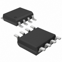
MAX412ESA Maxim Integrated Products, MAX412ESA Datasheet - Page 11

MAX412ESA
Manufacturer Part Number
MAX412ESA
Description
IC OPAMP DUAL28MHZ LOWNOISE8SOIC
Manufacturer
Maxim Integrated Products
Datasheet
1.MAX410CSA.pdf
(13 pages)
Specifications of MAX412ESA
Amplifier Type
General Purpose
Number Of Circuits
2
Slew Rate
4.5 V/µs
Gain Bandwidth Product
28MHz
Current - Input Bias
80nA
Voltage - Input Offset
120µV
Current - Supply
2.5mA
Current - Output / Channel
35mA
Voltage - Supply, Single/dual (±)
4.8 V ~ 10.5 V, ±2.4 V ~ 5.25 V
Operating Temperature
-40°C ~ 85°C
Mounting Type
Surface Mount
Package / Case
8-SOIC (3.9mm Width)
Lead Free Status / RoHS Status
Contains lead / RoHS non-compliant
Output Type
-
-3db Bandwidth
-
Available stocks
Company
Part Number
Manufacturer
Quantity
Price
Part Number:
MAX412ESA
Manufacturer:
MIAXM
Quantity:
20 000
Company:
Part Number:
MAX412ESA+T
Manufacturer:
BPS
Quantity:
12 000
On TDFN packages, there is an exposed paddle that
does not carry any current but should be connected to
V- (not the GND plane) for rated power dissipation.
Although the MAX410/MAX412/MAX414 are specified
with ±5V power supplies, they are also capable of sin-
gle-supply operation with voltages as low as 4.8V. The
minimum input voltage range for normal amplifier oper-
ation is between V- + 1.5V and V+ - 1.5V. The minimum
room-temperature output voltage range (with 2kΩ load)
Figure 7a. Capacitive-Load Driving Circuit
Figure 7b. Driving a 0.015µF Load with a 10Ω Isolation Resistor
V
OUTPUT
IN
Total Supply Voltage Considerations
INPUT
1V/div
1V/div
TDFN Exposed Paddle Connection
D.U.T
______________________________________________________________________________________
499Ω
Single/Dual/Quad, 28MHz, Low-Noise,
1µs/div
MAX410
MAX412
MAX414
10Ω
R
I
V
T
A
S
= +25°C
= ±5V
Low-Voltage, Precision Op Amps
C
L
> 0.015µF
GND
V
GND
OUT
is between V+ - 1.4V and V- + 1.3V for total supply volt-
ages between 4.8V and 10V. The output voltage range,
referenced to the supply voltages, decreases slightly
over temperature, as indicated in the ±5V Electrical
Characteristics tables. Operating characteristics at total
supply, voltages of less than 10V are guaranteed by
design and PSRR tests.
The offset null circuit of Figure 9 provides approximately
±450µV of offset adjustment range, sufficient for zeroing
offset over the full operating temperature range.
Figure 8. Capacitive-Load Driving Circuit with Loop-Enclosed
Isolation Resistor
Figure 9. MAX410 Offset Null Circuit
V
IN
909Ω
1kΩ
1
NULL
MAX410 Offset Voltage Null
D.U.T
82pF
C
F
10kΩ
10kΩ
MAX410
MAX410
MAX412
MAX414
NULL
10Ω
R
V+
I
8
7
C
0.01µF
L
V
OUT
11


