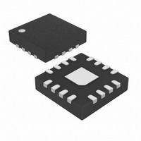
MAX4206ETE+ Maxim Integrated Products, MAX4206ETE+ Datasheet - Page 12

MAX4206ETE+
Manufacturer Part Number
MAX4206ETE+
Description
IC AMP TRANS LOG 16-TQFN
Manufacturer
Maxim Integrated Products
Datasheet
1.MAX4206ETET.pdf
(17 pages)
Specifications of MAX4206ETE+
Amplifier Type
Logarithmic
Number Of Circuits
1
Slew Rate
12 V/µs
Gain Bandwidth Product
5MHz
Voltage - Input Offset
1000µV
Current - Supply
5mA
Current - Output / Channel
58mA
Voltage - Supply, Single/dual (±)
2.7 V ~ 11 V, ±2.7 V ~ 5.5 V
Operating Temperature
-40°C ~ 85°C
Mounting Type
Surface Mount
Package / Case
16-TQFN Exposed Pad
Number Of Channels
1
Input Offset Voltage
5 mV
Operating Supply Voltage
3 V, 5 V, 9 V
Supply Current
5 mA
Operating Temperature Range
+ 85 C
Mounting Style
SMD/SMT
Power Dissipation
1349 mW
Lead Free Status / RoHS Status
Lead free / RoHS Compliant
Output Type
-
-3db Bandwidth
-
Current - Input Bias
-
Lead Free Status / Rohs Status
Details
Precision Transimpedance Logarithmic
Amplifier with Over 5 Decades of Dynamic Range
I
nificantly smaller than I
be eliminated:
Expanding this expression:
The first term of this expression is the ideal component
of V
In the second term, one can generally remove the
products relating to ∆K, because ∆K is generally much
less than 1. Hence, a good approximation for TE is
given by:
As an example, consider the following situation:
Full-scale input = 5V
I
I
K = 1 ±5% V/decade (note that the uncommitted ampli-
fier is configured for a gain of 4)
V
istics table)
V
T
Substituting into the total error approximation,
As a worst case, one finds TE ≅ ±178mV or ±3.6% of
full scale.
When expressed as a voltage, TE increases in proportion
with an increase in gain as the contributing errors are
defined at a specific gain. Calibration using a look-up
table eliminates the effects of gain and output offset
errors, leaving conformity error as the only factor con-
12
BIAS1
LOG
REF
A
LC
OSOUT
V
V
TE
TE
= +25°C
LOGV
LOGV
LOGV1
______________________________________________________________________________________
= 100nA
= ±5mV (obtained from the Electrical Character-
TE ≅ ± (1V/decade)(0.05log
= 100µA
≅ ±
≅ ±
and I
K
2
K K
= ±2mV (typ)
2
∆
. The remainder of the expression is the TE:
≅
≅
∆ log
±4 (±5mV ±2mV) = ±[0.15V ±4(±7mV)]
±
BIAS2
K
K
K
log
4 1
(
log
1
K
±
(
10
10
10
∆
±
are currents in the order of 20pA, sig-
K
∆
I
) log
I
LOG
I
I
REF
LOG
I
REF
K
I
LOG
REF
)
LOG
(
±
10
±
±
V
±
LC
4 1
and I
K K
I
I
LOG
4
REF
K
∆
±
(
(
±
V
V
OSOUT
±
log
REF
± ±
LC
∆
K
10
4
±
, and can therefore
10
)
(
(
V
±
OSOUT
I
)
I
(100µA/100nA)
LOG
V
V
REF
LC
LC
±
±
V
V
)
OSOUT
OSOUT
)
)
tributing to total error. For further accuracy, consider tem-
perature monitoring as part of the calibration process.
Five decades of input current across a 10nA to 1mA
range are acceptable for I
leakage currents increase as I
10nA. Bandwidth decreases at low I
the Frequency Response and Noise Considerations
section). As I
transistors become less logarithmic in nature. The
MAX4206 incorporates leakage current compensation
and high-current correction circuits to compensate for
these errors.
The MAX4206’s frequency response is a function of the
input current magnitude and the selected compensation
network at LOGIIN and REFIIN. The compensation net-
work comprised of C
over the specified range of input currents by introducing
an additional pole/zero to the system. For the typical
application, select C
Where high bandwidth at low current is required, C
= 32pF and R
sation values.
Figure 4. Ideal Transfer Function with Varying I
-0.5
-1.0
-1.5
1.5
1.0
0.5
0
1n
LOG
I
COMP
REF
Applications Information
IDEAL TRANSFER FUNCTION
10n
= 10nA
and I
COMP
COMP
WITH VARYING I
Frequency Compensation
= 330Ω are suitable compen-
100n
REF
I
REF
= 100pF and R
LOG
I
and R
LOG
= 1µA
increase to 1mA or higher,
1µ
Input Current Range
(A)
LOG
and I
10µ
COMP
REF
I
REF
and I
REF
= 100µA
100µ
LOG
ensures stability
. The effects of
REF
COMP
REF
1m
values (see
fall below
= 100Ω.
COMP


