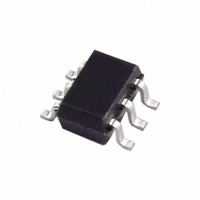
AD8029AKS-REEL Analog Devices Inc, AD8029AKS-REEL Datasheet - Page 15

AD8029AKS-REEL
Manufacturer Part Number
AD8029AKS-REEL
Description
IC AMP GP R-R LP 170MA SC70-6
Manufacturer
Analog Devices Inc
Datasheet
1.AD8029ARZ.pdf
(20 pages)
Specifications of AD8029AKS-REEL
Rohs Status
RoHS non-compliant
Amplifier Type
General Purpose
Number Of Circuits
1
Output Type
Rail-to-Rail
Slew Rate
63 V/µs
-3db Bandwidth
125MHz
Current - Input Bias
1.7µA
Voltage - Input Offset
2000µV
Current - Supply
1.4mA
Current - Output / Channel
170mA
Voltage - Supply, Single/dual (±)
2.7 V ~ 12 V, ±1.35 V ~ 6 V
Operating Temperature
-40°C ~ 125°C
Mounting Type
Surface Mount
Package / Case
SC-70-6, SC-88, SOT-363
Gain Bandwidth Product
-
THEORY OF OPERATION
The AD8029 (single), AD8030 (dual), and AD8040 (quad) are
rail-to-rail input and output amplifiers fabricated using Analog
Devices’ XFCB process. The XFCB process enables the AD8029/
AD8030/AD8040 to operate on 2.7 V to 12 V supplies with a
120 MHz bandwidth and a 60 V/µs slew rate. A simplified sche-
matic of the AD8029/AD8030/AD8040 is shown in Figure 50.
INPUT STAGE
For input common-mode voltages less than a set threshold
(1.2 V below V
(comprising Q
the input voltage to go 200 mV below –V
common-mode voltages exceeding the same threshold cause
I
the NPN differential pair through transistor Q
condition, the input common-mode voltage is allowed to rise
200 mV above +V
behavior. The transition between these two modes of operation
leads to a sudden, temporary shift in input stage transconduc-
tance, g
V
The SPD block shortens the duration of this transition, thus
improving the distortion performance. As shown in Figure 50,
the input differential pair is protected by a pair of two series
diodes, connected in anti-parallel, which clamp the differential
input voltage to approximately ±1.5 V.
TAIL
OS
), which in turn adversely affect the distortion performance.
to be routed away from the PNP differential pair and into
m
, and dc parameters (such as the input offset voltage
DISABLE
1
AD8029 ONLY
CC
toQ
), the resistor degenerated PNP differential pair
IN–
IN+
S
while still maintaining linear amplifier
4
) carries the entire I
TO DISABLE
CIRCUITRY
TAIL
S
. Conversely, input
current, allowing
Q
9
. Under this
5
R
5
R
6
OUT
Q
Q
R
+V
6
7
Figure 50. Simplified Schematic
7
R
I
–V
TH
TH
S
R
S
–1.2V
COM
8
Rev. A | Page 15 of 20
Q
8
IN
Q
9
SPD
Q
R
1
1
R
2
OUTPUT STAGE
The currents derived from the PNP and NPN input differential
pairs are injected into the current mirrors M
establishing a common-mode signal voltage at the input of the
output buffer.
The output buffer performs three functions:
1.
2.
3.
The output devices Q
configuration, and are Miller-compensated by internal
capacitors, C
The output voltage compliance is set by the output devices’
collector resistance R
current I
output voltage to swing to within 40 mV of either rail, while
heavier loads cause this figure to deteriorate as R
Q
2
Q
R
3
3
I
It buffers and applies the desired signal voltage to the
output devices, Q
It senses the common-mode current level in the output
devices.
It regulates the output common-mode current by
establishing a common-mode feedback loop.
TAIL
R
4
Q
4
L
. For instance, a light equivalent load (5 kΩ) allows the
MT
and C
M
M
TOP
BOT
C
10
MB
10
(about 25 Ω), and by the required load
and Q
.
and Q
AD8029/AD8030/AD8040
OUTPUT
BUFFER
11
11
work in a common-emitter
.
C
C
MT
MB
Q
Q
BOT
10
11
03679-0-051
+V
V
–V
and M
OUT
C
S
S
× I
L
.
TOP
, thus


