NJM2143R-TE1 NJR, NJM2143R-TE1 Datasheet
首页 Integrated Circuits (ICs) Linear - Amplifiers - Instrumentation, OP Amps, Buffer Amps NJM2143R-TE1
Manufacturer Part Number
NJM2143R-TE1
Description
IC OPAMP DUAL SNGL-SUPPLY 8-VSP
Specifications of NJM2143R-TE1
Amplifier Type
General Purpose
Number Of Circuits
2
Slew Rate
0.5 V/µs
Gain Bandwidth Product
600kHz
Current - Input Bias
25nA
Voltage - Input Offset
2000µV
Current - Supply
700µA
Current - Output / Channel
30mA
Voltage - Supply, Single/dual (±)
3 V ~ 20 V
Operating Temperature
-40°C ~ 85°C
Mounting Type
Surface Mount
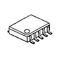
Package / Case
8-VSP
Number Of Channels
2
Voltage Gain Db
100 dB
Common Mode Rejection Ratio (min)
85 dB
Input Offset Voltage
7 mV
Operating Supply Voltage
5 V, 9 V, 12 V, 15 V, 18 V
Supply Current
1.2 mA
Maximum Power Dissipation
320 mW
Maximum Operating Temperature
+ 85 C
Mounting Style
SMD/SMT
Minimum Operating Temperature
- 40 C
Lead Free Status / RoHS Status
Contains lead / RoHS non-compliant
Output Type
-
-3db Bandwidth
-
Lead Free Status / Rohs Status
Details
Available stocks
Part Number:
NJM2143R-TE1
■ GENERAL DESCRIPTION
VSP8.Its input stage of Darlington PNP detects GND level.
the load is direct-coupled to ground.
■ FEATURES
■ PIN CONFIGURATION
■ EQUIVALENT CIRCUIT ( 1/2 Shown )
Ver.2003-03-17
● Single-Supply Operation
● Operating Voltage
● Low Operating Current
● Bipolar Technology
● Package Outline
The NJM2143 is a single-supply operational amplifier in
There is no crossover distortion in single supply operation when
SINGLE-SUPPLY DUAL OPERATIONAL AMPLIFIER
( +3~+20V )
( 0.7mA typ. )
VSP8,TVSP8
( Top View )
■ PACKAGE OUTLINE
PIN FUNCTION
1.A OUTPUT
2.A –INPUT
3.A +INPUT
4.GND
5.B +INPUT
6.B –INPUT
7.B OUTPUT
8.V
+
NJM2143R
NJM2143RB1
- 1 -
Related parts for NJM2143R-TE1
NJM2143R-TE1 Summary of contents
... Bipolar Technology ● Package Outline ■ PIN CONFIGURATION ■ EQUIVALENT CIRCUIT ( 1/2 Shown ) Ver.2003-03-17 ■ PACKAGE OUTLINE ( +3~+20V ) ( 0.7mA typ. ) VSP8,TVSP8 ( Top View ) PIN FUNCTION 1.A OUTPUT 2.A –INPUT 3.A +INPUT 4.GND 5.B +INPUT 6.B –INPUT 7.B OUTPUT 8.V NJM2143R NJM2143RB1 + - 1 - ...
ABSOLUTE MAXIMUM RATINGS PARAMETER Supply Voltage Differential Input Voltage Input Voltage Power Dissipation Operating Temperature Range Storage Temperature Range ( note1 ) When input voltage is less than +20V, the absolute maximum control voltage is equal to the input ...
TYPICAL CHARACTERISTICS Ver.2003-03- ...
TYPICAL CHARACTERISTICS - 4 - Ver.2003-03-17 ...
TYPICAL CHARACTERISTICS Ver.2003-03-17 [CAUTION] The specifications on this databook are only given for information , without any guarantee as regards either mistakes or omissions. The application circuits in this databook are described only to show representative usages of the ...
Related keywords
njm2122 njm2100 njm2121 njm2140r njm2140 njm2115 njm2114 njm2100d njm2147m njm2147 njm2146b njm2114m NJM2143R-TE1 datasheet NJM2143R-TE1 data sheet NJM2143R-TE1 pdf datasheet NJM2143R-TE1 component NJM2143R-TE1 part NJM2143R-TE1 distributor NJM2143R-TE1 RoHS NJM2143R-TE1 datasheet download