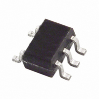
AD8515AKS-R2 Analog Devices Inc, AD8515AKS-R2 Datasheet - Page 13

AD8515AKS-R2
Manufacturer Part Number
AD8515AKS-R2
Description
IC AMP GP R-R CMOS 5MHZ SC70-5
Manufacturer
Analog Devices Inc
Datasheet
1.AD8515ARTZ-REEL7.pdf
(16 pages)
Specifications of AD8515AKS-R2
Rohs Status
RoHS non-compliant
Design Resources
Extending the Capacitive Input Range of AD7745/AD7746 (CN0129)
Amplifier Type
General Purpose
Number Of Circuits
1
Output Type
Rail-to-Rail
Slew Rate
2.7 V/µs
Gain Bandwidth Product
5MHz
Current - Input Bias
5pA
Voltage - Input Offset
1000µV
Current - Supply
410µA
Current - Output / Channel
20mA
Voltage - Supply, Single/dual (±)
1.8 V ~ 5 V
Operating Temperature
-40°C ~ 125°C
Mounting Type
Surface Mount
Package / Case
SC-70-5, SC-88A, SOT-323-5, SOT-353, 5-TSSOP
-3db Bandwidth
-
Other names
AD8515AKS-R2
AD8515AKS-R2TR
AD8515AKS-R2TR
DRIVING CAPACITIVE LOADS
Most amplifiers have difficulty driving large capacitive loads.
Additionally, higher capacitance at the output can increase the
amount of overshoot and ringing in the amplifier’s step response
and can even affect the stability of the device. This is due to the
degradation of phase margin caused by additional phase lag from
the capacitive load. The value of capacitive load that an amplifier
can drive before oscillation varies with gain, supply voltage, input
signal, temperature, and other parameters. Unity gain is the most
challenging configuration for driving capacitive loads. The AD8515
is capable of driving large capacitive loads without any external
compensation. The graphs in Figure 31 and Figure 32 show the
amplifier’s capacitive load driving capability when configured
in unity gain of +1.
The AD8515 is even capable of driving higher capacitive loads
in inverting gain of −1, as shown in Figure 33.
Figure 32. Capacitive Load Driving @ C
Figure 31. Capacitive Load Driving @ C
TIME (1µs/DIV)
TIME (1µs/DIV)
L
L
= 500 pF
= 50 pF
V
C
GAIN = 1
V
C
GAIN = 1
S
L
S
L
= ±2.5V
= 50pF
= ±2.5V
= 500pF
Rev. D | Page 13 of 16
FULL POWER BANDWIDTH
The slew rate of an amplifier determines the maximum frequency
at which it can respond to a large input signal. This frequency
(known as full power bandwidth, FPBW) can be calculated from
the equation
for a given distortion. The FPBW of the AD8515 is shown in
Figure 34 to be close to 200 kHz.
FPBW
Figure 33. Capacitive Load Driving @ C
=
2
V
V
IN
OUT
π
×
Figure 34. Full Power Bandwidth
SR
V
PEAK
TIME (1µs/DIV)
TIME (2µs/DIV)
L
= 800 pF
V
C
GAIN = –1
S
L
= ±0.9V
= 800pF
AD8515


