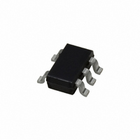
CLC406AJM5 National Semiconductor, CLC406AJM5 Datasheet

CLC406AJM5
Specifications of CLC406AJM5
Related parts for CLC406AJM5
CLC406AJM5 Summary of contents
Page 1
... National’s proven current feedback architec- tures, the CLC406 is available in several versions to meet a variety of requirements. Connection Diagrams Pinout DIP & SOIC © 2001 National Semiconductor Corporation Features n 160MHz small signal bandwidth n 50mW power ( ± 5V supplies, the n 0.02%/0.02˚ differential gain/phase n 12ns settling to 0.05% n 1500V/µ ...
Page 2
... Ordering Information Package 8-pin plastic DIP 8-pin plastic SOIC 5-pin SOT www.national.com Temperature Range Part Number Industrial −40˚C to +85˚C CLC406AJP −40˚C to +85˚C CLC406AJE −40˚C to +85˚C CLC406AJM5 2 Package NSC Marking Drawing CLC406AJP N08E CLC406AJE M08A A17 MA05A ...
Page 3
... Absolute Maximum Ratings If Military/Aerospace specified devices are required, please contact the National Semiconductor Sales Office/Distributors for availability and specifications. Supply Voltage ( OUT Output is short circuit protected to ground, but maximum reliability will be maintained if I does not OUT exceed... Common Mode Input Voltage ...
Page 4
Electrical Characteristics ± + 5V, R =100 , Symbol Parameter Distortion And Noise Response ICN Inverting Current NCN Non Inverting Current SNF Total Noise Floor INV Total Integrated Noise Static, DC ...
Page 5
Typical Performance Characteristics less specified Non-Inverting Frequency Response Large Signal Inverting Frequency Response Short-Term Settling Time T = 25˚ +6V Inverting Frequency Response DS012747-1 Small Signal Pulse Response DS012747-3 Long-Term Settling Time DS012747-18 5 ± ...
Page 6
Typical Performance Characteristics unless specified (Continued) Harmonic Distortion R and Settling Time vs. Capacitive Load s 3rd Harmonic Distortion vs. Output Power www.national.com T = 25˚ +6V 2-Tone, 3rd Order, Spurious Levels DS012747-4 2nd Harmonic ...
Page 7
Typical Performance Characteristics unless specified (Continued) Equivalent Input Noise Open-Loop Transimpedance Gain, Z( 25˚ +6V PSRR, CMRR, and Closed Loop R DS012747-10 DS012747-12 7 ± 100 , R = ...
Page 8
Application Division FIGURE 1. Recommended Non-Inverting Gain Circuit Feedback Resistor The CLC406 achieves its exceptional AC performance while requiring very low quiescent power by using the current feedback topology and an internal slew rate enhancement circuit. The loop gain and ...
Page 9
Application Division (Continued) generally higher and relatively insensitive to gain setting for inverting gain operation. An additional discussion of slew rates can be found in the CLC404 data sheet. As the output signal swing is increased, the slew enhancement circuit ...
Page 10
Physical Dimensions www.national.com inches (millimeters) unless otherwise noted 8-Pin MDIP NS Package Number N08E 8-Pin SOIC NS Package Number M08A 10 ...
Page 11
... NATIONAL’S PRODUCTS ARE NOT AUTHORIZED FOR USE AS CRITICAL COMPONENTS IN LIFE SUPPORT DEVICES OR SYSTEMS WITHOUT THE EXPRESS WRITTEN APPROVAL OF THE PRESIDENT AND GENERAL COUNSEL OF NATIONAL SEMICONDUCTOR CORPORATION. As used herein: 1. Life support devices or systems are devices or systems which, (a) are intended for surgical implant ...


