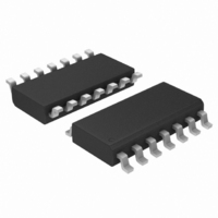
MC33204VDR2G ON Semiconductor, MC33204VDR2G Datasheet - Page 5

MC33204VDR2G
Manufacturer Part Number
MC33204VDR2G
Description
IC OPAMP QUAD R-R LO VOLT 14SOIC
Manufacturer
ON Semiconductor
Datasheet
1.MC33201PG.pdf
(18 pages)
Specifications of MC33204VDR2G
Amplifier Type
General Purpose
Number Of Circuits
4
Output Type
Rail-to-Rail
Slew Rate
1 V/µs
Gain Bandwidth Product
2.2MHz
Current - Input Bias
80nA
Voltage - Input Offset
10000µV
Current - Supply
1.125mA
Current - Output / Channel
80mA
Voltage - Supply, Single/dual (±)
1.8 V ~ 12 V, ±0.9 V ~ 6 V
Operating Temperature
-55°C ~ 125°C
Mounting Type
Surface Mount
Package / Case
14-SOIC (3.9mm Width), 14-SOL
Number Of Channels
4
Voltage Gain Db
109.54 dB
Common Mode Rejection Ratio (min)
60 dB
Input Voltage Range (max)
Positive Rail
Input Voltage Range (min)
Negative Rail
Input Offset Voltage
17 mV
Operating Supply Voltage
12 V
Supply Current
3.6 mA
Maximum Operating Temperature
+ 125 C
Mounting Style
SMD/SMT
Maximum Dual Supply Voltage
+/- 6 V
Minimum Operating Temperature
- 55 C
Lead Free Status / RoHS Status
Lead free / RoHS Compliant
-3db Bandwidth
-
Lead Free Status / Rohs Status
Details
Other names
MC33204VDR2GOS
MC33204VDR2GOS
MC33204VDR2GOSTR
MC33204VDR2GOS
MC33204VDR2GOSTR
Available stocks
Company
Part Number
Manufacturer
Quantity
Price
Company:
Part Number:
MC33204VDR2G
Manufacturer:
ON Semiconductor
Quantity:
5 150
Part Number:
MC33204VDR2G
Manufacturer:
ON/安森美
Quantity:
20 000
- 200
- 250
-100
-150
2500
2000
1500
1000
- 50
150
100
500
10
50
50
40
30
20
- 55 - 40 - 25
- 50
0
0
0
0
TC
8 and 14 Pin DIP Pkg
V
- 40
IO
Figure 2. Maximum Power Dissipation
, INPUT OFFSET VOLTAGE TEMPERATURE COEFFICIENT ( m V/ ° C)
Temperature Coefficient Distribution
SOIC-8
2.0
Pkg
- 30
V
versus Common Mode Voltage
Figure 4. Input Offset Voltage
CM
Figure 6. Input Bias Current
, INPUT COMMON MODE VOLTAGE (V)
T
- 20
A
, AMBIENT TEMPERATURE (°C)
versus Temperature
4.0
0
-10
TSSOP-14 Pkg
25
6.0
0
SO-14 Pkg
10
50
360 amplifiers tested from
3 (MC33204) wafer lots
8.0
V
V
T
DIP Package
A
CC
EE
20
= 25°C
= Gnd
= + 5.0 V
85
30
V
V
T
A
CC
EE
10
= 25°C
= Gnd
= 12 V
http://onsemi.com
40
125
50
12
5
200
160
120
300
260
220
180
140
100
5.0
30
25
20
15
10
40
35
80
40
- 55 - 40 - 25
- 55 - 40 - 25
0
-10
0
V
V
R
DV
- 8.0
Figure 3. Input Offset Voltage Distribution
Figure 7. Open Loop Voltage Gain versus
CC
EE
L
= 600 W
O
= Gnd
= + 5.0 V
= 0.5 V to 4.5 V
- 6.0
Figure 5. Input Bias Current
V
V
T
T
- 4.0
IO
CM
A
A
, AMBIENT TEMPERATURE (°C)
, AMBIENT TEMPERATURE (°C)
, INPUT OFFSET VOLTAGE (mV)
versus Temperature
> 1.0 V
0
0
- 2.0
Temperature
25
25
0
V
CM
2.0
= 0 V to 0.5 V
70
70
360 amplifiers tested from
3 (MC33204) wafer lots
V
V
T
DIP Package
A
CC
EE
4.0
= 25°C
V
V
= Gnd
= + 5.0 V
CC
EE
6.0
= Gnd
= + 5.0 V
85
85
8.0
105
125
125
10


