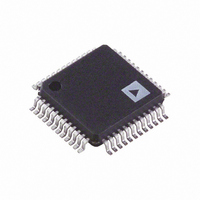
ADM1062ASUZ Analog Devices Inc, ADM1062ASUZ Datasheet - Page 27

ADM1062ASUZ
Manufacturer Part Number
ADM1062ASUZ
Description
IC SUPERVISOR/SEQUENCER 48-TQFP
Manufacturer
Analog Devices Inc
Type
Sequencerr
Datasheet
1.EVAL-ADM1062LFEB.pdf
(36 pages)
Specifications of ADM1062ASUZ
Number Of Voltages Monitored
10
Output
Programmable
Voltage - Threshold
Adjustable/Selectable
Operating Temperature
-40°C ~ 85°C
Mounting Type
Surface Mount
Package / Case
48-TQFP, 48-VQFP
For Use With
EVAL-ADM1062TQEBZ - BOARD EVALUATION FOR ADM1062TQEVAL-ADM1062LFEBZ - BOARD EVALUATION FOR ADM1062LF
Lead Free Status / RoHS Status
Lead free / RoHS Compliant
Reset
-
Reset Timeout
-
Available stocks
Company
Part Number
Manufacturer
Quantity
Price
Company:
Part Number:
ADM1062ASUZ
Manufacturer:
Analog Devices Inc
Quantity:
10 000
Part Number:
ADM1062ASUZ
Manufacturer:
ADI/亚德诺
Quantity:
20 000
Company:
Part Number:
ADM1062ASUZ-REEL7
Manufacturer:
Analog Devices Inc
Quantity:
10 000
UPDATING THE SEQUENCING ENGINE
Sequencing engine (SE) functions are not updated in the same way
as regular configuration latches. The SE has its own dedicated
512-byte nonvolatile, electrically erasable, programmable, read-
only memory (EEPROM) for storing state definitions. The
EEPROM provides 63 individual states, each with a 64-bit word
(one state is reserved). At power-up, the first state is loaded from
the SE EEPROM into the engine itself. When the conditions of this
state are met, the next state is loaded from the EEPROM into the
engine, and so on. The loading of each new state takes approxi-
mately 10 μs.
To alter a state, the required changes must be made directly to
the EEPROM. RAM for each state does not exist. The relevant
alterations must be made to the 64-bit word, which is then
uploaded directly to the EEPROM.
INTERNAL REGISTERS
The ADM1062 contains a large number of data registers. The
principal registers are the address pointer register and the
configuration registers.
Address Pointer Register
The address pointer register contains the address that selects
one of the other internal registers. When writing to the ADM1062,
the first byte of data is always a register address that is written to
the address pointer register.
Configuration Registers
The configuration registers provide control and configuration
for various operating parameters of the ADM1062.
EEPROM
The ADM1062 has two 512-byte cells of nonvolatile EEPROM
from Register Address 0xF800 to Register Address 0xFBFF. The
EEPROM is used for permanent storage of data that is not lost
when the ADM1062 is powered down. One EEPROM cell contains
the configuration data of the device; the other contains the state
definitions for the SE. Although referred to as read-only memory,
the EEPROM can be written to, as well as read from, using the
serial bus in exactly the same way as the other registers.
(V
POWER-UP
EEPROM
CC
> 2.5V)
M
E
E
P
R
O
L
D
CONTROLLER
Figure 38. Configuration Update Flow Diagram
D
A
A
T
DEVICE
SMBus
LATCH A
Rev. B | Page 27 of 36
M
R
A
L
D
U
P
D
The major differences between the EEPROM and other
registers are as follows:
•
•
•
The first EEPROM is split into 16 (0 to 15) pages of 32 bytes
each. Page 0 to Page 6, starting at Address 0xF800, hold the
configuration data for the applications on the ADM1062 (such
as the SFDs and PDOs). These EEPROM addresses are the same
as the RAM register addresses, prefixed by F8. Page 7 is reserved.
Page 8 to Page 15 are for customer use.
Data can be downloaded from the EEPROM to the RAM in one
of the following ways:
•
•
SERIAL BUS INTERFACE
The ADM1062 is controlled via the serial system management
bus (SMBus) and is connected to this bus as a slave device under
the control of a master device. It takes approximately 1 ms after
power-up for the ADM1062 to download from its EEPROM.
Therefore, access to the ADM1062 is restricted until the download
is complete.
Identifying the ADM1062 on the SMBus
The ADM1062 has a 7-bit serial bus slave address (see Table 12).
The device is powered up with a default serial bus address. The
five MSBs of the address are set to 00101; the two LSBs are
determined by the logical states of Pin A1 and Pin A0. This
allows the connection of four ADM1062s to one SMBus.
Table 12. Serial Bus Slave Address
A1 Pin
Low
Low
High
High
1
x = Read/Write bit. The address is shown only as the first 7 MSBs.
An EEPROM location must be blank before it can be
written to. If it contains data, the data must first be erased.
Writing to the EEPROM is slower than writing to the RAM.
Writing to the EEPROM should be restricted because it has
a limited write/cycle life of typically 10,000 write operations
due to the usual EEPROM wear-out mechanisms.
At power-up, when Page 0 to Page 6 are downloaded
By setting Bit 0 of the UDOWNLD register (0xD8), which
performs a user download of Page 0 to Page 6
LATCH B
A0 Pin
Low
High
Low
High
(OV THRESHOLD
FUNCTION
ON VP1)
Hex Address
0x28
0x2A
0x2C
0x2E
7-Bit Address
0010100x
0010101x
0010110x
0010111x
ADM1062
1
1
1
1


