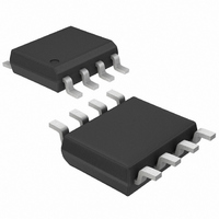
MAX814TCSA+ Maxim Integrated Products, MAX814TCSA+ Datasheet - Page 14

MAX814TCSA+
Manufacturer Part Number
MAX814TCSA+
Description
IC SUPERVISOR MPU LP 8SOIC
Manufacturer
Maxim Integrated Products
Type
Simple Reset/Power-On Resetr
Datasheet
1.MAX814NCPA.pdf
(16 pages)
Specifications of MAX814TCSA+
Number Of Voltages Monitored
1
Output
Push-Pull, Push-Pull
Reset
Active High/Active Low
Reset Timeout
140 ms Minimum
Voltage - Threshold
3.03V
Operating Temperature
0°C ~ 70°C
Mounting Type
Surface Mount
Package / Case
8-SOIC (3.9mm Width)
Monitored Voltage
1 V to 5.5 V
Output Type
Active High, Active Low, Push-Pull
Manual Reset
Resettable
Watchdog
No Watchdog
Battery Backup Switching
No Backup
Supply Voltage (max)
5.5 V
Supply Voltage (min)
1 V
Supply Current (typ)
75 uA
Maximum Power Dissipation
471 mW
Maximum Operating Temperature
+ 70 C
Mounting Style
SMD/SMT
Minimum Operating Temperature
0 C
Power Fail Detection
Yes
Undervoltage Threshold
3 V
Overvoltage Threshold
3.06 V
Power-up Reset Delay (typ)
250 ms
Lead Free Status / RoHS Status
Lead free / RoHS Compliant
±1% Accuracy, Low-Power, +3V and +5V
µP Supervisory Circuits
Figure 12. Monitoring a Negative Voltage
Figure 13. Flow Chart of WDI Implementation
14
+5V
V-
PFO
MR
______________________________________________________________________________________
R1
R2
+5V
+5V
0V
0V
V
PFT
5 - 2.5
= 2.5V (K, L, N); 1.70V (T AND MAX816)
R1
=
2.5 - V
R2
YES
V-
PFI
TRIP ,
BEGIN PROGRAM
MAX814
MAX815
MAX816
SUBROUTINE
V
SET LOW
SET HIGH
TRIP
SET LOW
RETURN
GND
V
WDI
WDI
CC
WDI
< 0V
NO
V
RESET
TRIP
PFO
MR
100kΩ
0V
TO µP
2N3904
100kΩ
In addition to issuing a reset to the µP during power-up,
power-down, and brownout conditions, the MAX814/
MAX815/MAX816 series is relatively immune to short
duration negative-going V
Typical Operating Characteristics show a graph of
Maximum Transient Duration vs. Reset Comparator
Overdrive, for which a reset is not generated. The
graph was made using a negative-going pulse applied
to V
and ending below it by the magnitude indicated (reset
comparator overdrive). The graph indicates the typical
maximum pulse width a negative-going V
may have without causing a reset pulse. As the magni-
tude of the transient increases (goes further below the
reset threshold), the maximum allowable pulse width
decreases. Typically, a V
reset threshold and lasts 30µs or less will not cause a
reset pulse to be issued.
A 0.1µF bypass capacitor mounted as close as possible
to pin 2 (V
µPs with bidirectional reset pins, such as the Motorola
68HC11 series, can cause a conflict with the RESET
output. If, for example, the RESET output is driven high
and the µP wants to pull it low, indeterminate logic lev-
els may result. To correct this, connect a 4.7kΩ resistor
between the RESET output and the µP reset I/O, as in
Figure 14. Buffer the RESET output to other system
components.
Figure 14. Interfacing to µPs with Bidirectional Reset I/O
CC
, starting 1.5V above the actual reset threshold
MAX814
MAX815
MAX816
GND
V
CC
CC
) provides additional transient immunity.
RESET
Negative-Going V
with Bidirectional Reset Pins
BUFFERED RESET TO OTHER SYSTEM COMPONENTS
4.7kΩ
CC
CC
that goes 100mV below the
transients (glitches). The
Interfacing to µPs
RESET
CC
Transients
GND
V
µP
CC
CC
transient


