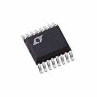
LTC2901-4CGN#TR Linear Technology, LTC2901-4CGN#TR Datasheet - Page 12

LTC2901-4CGN#TR
Manufacturer Part Number
LTC2901-4CGN#TR
Description
IC MONITOR QUAD SUPP PROG 16SSOP
Manufacturer
Linear Technology
Type
Multi-Voltage Supervisorr
Datasheet
1.LTC2901-3CGNPBF.pdf
(16 pages)
Specifications of LTC2901-4CGN#TR
Number Of Voltages Monitored
4
Output
Push-Pull, Totem Pole
Reset
Active Low
Reset Timeout
5 ms Minimum
Voltage - Threshold
16 Selectable Threshold Combinations
Operating Temperature
0°C ~ 70°C
Mounting Type
Surface Mount
Package / Case
16-SSOP
Lead Free Status / RoHS Status
Contains lead / RoHS non-compliant
Available stocks
Company
Part Number
Manufacturer
Quantity
Price
APPLICATIO S I FOR ATIO
LTC2901
In a negative adjustable application, the minimum value
for R4 is limited by the sourcing capability of V
With no other load on V
Tables 2 and 3 offer suggested 1% resistor values for
various adjustable applications.
Once the resistor divider is set in the 5% tolerance mode
(LTC2901-3/LTC2901-4), there is no need to change the
divider for the 10% mode because the internal and exter-
nal reference is scaled accordingly, moving the trip point
by –5%.
Although all four supply monitor comparators have built-
in glitch immunity, bypass capacitors on V1 and V2 are
recommended because the greater of V1 or V2 is also the
V
inputs are allowed.
Power-Down
On power-down, once any of the V
their threshold, RST and COMPX are held at a logic low.
A logic low of 0.4V is guaranteed until both V1 and V2
drop below 1V. If the bandgap reference becomes invalid
12
CC
1.21V ÷ 1mA = 1.21kΩ.
for the device. Filter capacitors on the V3 and V4
Figure 6. Setting the Negative Adjustable Trip Point
Figure 5. Setting the Positive Adjustable Trip Point
V3 OR V4
V
TRIP
R4
1%
R3
1%
V
TRIP
R3
1%
R4
1%
12
13
U
V
V4
REF
REF
U
+
–
, R4 (minimum) is:
–
+
0.5V
LTC2901
+
–
LTC2901
W
X
inputs drop below
2901 F06
2901 F05
REF
U
(±1mA).
Table 2. Suggested 1% Resistor Values for the ADJ Inputs
Table 3. Suggested 1% Resistor Values for the –ADJ Input
(V
above 2.4V max.
Monitor Output Rise and Fall Time Estimation
All of the outputs (RST, COMPX, WDO) have strong pull-
down capability. If the external load capacitance (C
for a particular output is known, output fall time (10% to
90%) is estimated using:
where R
transistor. The typical performance curve (V
demonstrates that the pull-down current is somewhat
linear versus output voltage. Using the 25°C curve, R
estimated to be approximately 40Ω. Assuming a 150pF
load capacitance, the fall time is about 13.2ns.
Although the outputs are considered to be “open-drain,”
they do have a weak pull-up capability (see COMPX or RST
CC
V
V
t
FALL
SUPPLY
SUPPLY
–5.2
< 2V typ), the part will reprogram once V
–10
–12
7.5
3.3
2.5
1.8
1.5
1.2
0.9
–2
–5
12
10
8
6
5
3
1
≈ 2.2 • R
PD
(V)
(V)
is the on-resistance of the internal pull-down
PD
V
V
–11.30
TRIP
TRIP
11.25
4.725
3.055
2.325
1.685
1.410
1.120
0.933
0.840
–1.87
–4.64
–4.87
–9.31
2.82
9.4
7.5
5.6
• C
7
(V)
(V)
LOAD
R3 (kΩ)
R3 (kΩ)
2150
1780
1400
1300
1020
1130
86.6
68.1
845
511
464
365
237
182
124
187
464
487
931
OL
R4 (kΩ)
R4 (kΩ)
100
100
100
100
100
100
100
100
100
100
100
100
100
100
121
121
121
121
121
vs I
CC
LOAD
rises
SINK
PD
2901fb
is
)
)


