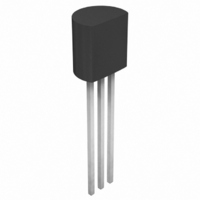
S-80850CNY-B-G Seiko Instruments, S-80850CNY-B-G Datasheet - Page 23

S-80850CNY-B-G
Manufacturer Part Number
S-80850CNY-B-G
Description
IC VOLT DETECTOR 5.0V TO-92
Manufacturer
Seiko Instruments
Type
Simple Reset/Power-On Resetr
Datasheet
1.S-80821CNMC-B8GT2G.pdf
(59 pages)
Specifications of S-80850CNY-B-G
Number Of Voltages Monitored
1
Output
Open Drain or Open Collector
Reset
Active Low
Voltage - Threshold
5V
Operating Temperature
-40°C ~ 85°C
Mounting Type
Through Hole
Package / Case
TO-92-3 (Standard Body), TO-226
Output Type
Open Collector / Drain
Undervoltage Threshold
5.0 V
Power-up Reset Delay (typ)
Adj
Supply Voltage (min)
0.95 V
Supply Voltage (max)
10 V
Supply Current (typ)
0.8 uA
Operating Temperature Range
- 40 C to + 85 C
Mounting Style
Through Hole
Description/function
Two output forms, Nch open-drain and CMOS output
Detection Range
5 V +/- 2 %
Internal Hysteresis
Yes
Manual Reset
No
Operating Supply Voltage
0.95 V to 10 V
Watchdog
No
Lead Free Status / RoHS Status
Lead free / RoHS Compliant
Reset Timeout
-
Lead Free Status / Rohs Status
Lead free / RoHS Compliant
Rev.5.0
1. Basic Operation: CMOS Output (Active Low)
Operation
1-1. When the power supply voltage (V
1-2. When the V
1-3. When the V
1-4. The V
1-5. When the V
_00
OFF and the Pch transistor is ON to provide V
Figure 17 is OFF, the comparator input voltage is
the detection voltage −V
becomes ON, the Pch transistor becomes OFF, and the V
the Nch transistor N1 in Figure 17 becomes ON, the comparator input voltage is changed to
V
appears even when the V
transistor becomes ON to provide V
R
R
DD
B
A
•
+
when the output is pulled up to the V
V
SS
R
DD
B
level appears when the V
.
DD
DD
DD
SUPER-SMALL PACKAGE HIGH-PRECISION VOLTAGE DETECTOR
falls below the minimum operating voltage, the output becomes undefined, or goes to the
goes below +V
rises above +V
*1. Parasiteic diode
VDD
VSS
DET
DD
. When the V
surpasses −V
*1
DET
DET
V
REF
, the output provides the V
(point B in Figure 18 ), the Nch transistor becomes OFF and the Pch
DD
Seiko Instruments Inc.
DD
DD
Figure 17 Operation 1
) is higher than the release voltage (+V
rises above the minimum operating voltage. The V
R
R
R
A
level at the output.
B
C
DD
DD
DET
.
falls below −V
, as long as it does not exceed the release voltage +V
−
+
DD
(high) at the output. Since the Nch transistor N1 in
N1
R (
R
B
A
+
+
R
R
DET
SS
C
DD
B
)
+
•
level appears at the output. At this time
(point A in Figure 18 ), the Nch transistor
level, as long as the V
R
V
DD
C
Pch
Nch
.
*1
*1
DET
OUT
), the Nch transistor is
S-808xxC Series
DD
remains above
SS
level still
DET
23
.


