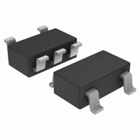
NCP301LSN11T1G ON Semiconductor, NCP301LSN11T1G Datasheet - Page 15

NCP301LSN11T1G
Manufacturer Part Number
NCP301LSN11T1G
Description
IC VOLTAGE DETECTOR 1.1V SOT23-5
Manufacturer
ON Semiconductor
Type
Simple Reset/Power-On Resetr
Datasheet
1.NCP300HSN47T1G.pdf
(26 pages)
Specifications of NCP301LSN11T1G
Number Of Voltages Monitored
1
Output
Open Drain or Open Collector
Reset
Active Low
Voltage - Threshold
1.1V
Operating Temperature
-40°C ~ 85°C
Mounting Type
Surface Mount
Package / Case
TSOT-23-5, TSOT-5, TSOP-5
Mounting Style
SMD/SMT
Lead Free Status / RoHS Status
Lead free / RoHS Compliant
Reset Timeout
-
Available stocks
Company
Part Number
Manufacturer
Quantity
Price
Company:
Part Number:
NCP301LSN11T1G
Manufacturer:
ON Semiconductor
Quantity:
2 100
monitoring
power−down, and brownout/sag conditions, and rejects
negative glitches on the power supply line. Figure 22 shows
the maximum transient duration vs. maximum negative
excursion (overdrive) for glitch rejection. Any combination
of duration and overdrive which lies under the curve will not
generate a reset signal. A below−V
right) is detected as a brownout or power−down. Typically,
any transient that goes 100 mV below the reset threshold and
lasts 5.0 ms or less will not cause a reset pulse.
capacitor in close proximity to the V
Figure 22. Max Transient Duration vs. Max Overdrive
The NCP300 and NCP301 series provides accurate V
Transient immunity can be improved by adding a
300
250
200
150
100
50
0
10
V
V
CC
TH
V
30
CC
RESET COMPARATOR OVERDRIVE
and
TRANSIENT REJECTION
50
reset
Duration
Figure 23.
V
TH
V
70
= 4.90 V
TH
timing
= 3.10 V
V
TH
90
= 1.60 V
CC
CC
during
110
pin of the NCP30x.
condition (on the
Overdrive
130
power−up,
150
http://onsemi.com
CC
15
and V
three major factors should be considered:
calculated as follows:
Where:
V
decreasing Vin
V
the data sheet to figure out the V
typical detection voltage reflected in the part number, the
threshold values are designed to the following targets (at
25°C):
By
Equations 2 to 6, Equation 1 becomes:
FACTORS TO BE CONSIDERED FOR VOLTAGE
Output
DET−_max
HYS_max
The following hysteresis graph depicts V
For selecting a voltage option in the NCP30X family,
The V
The above two parameters can be obtained directly from
In the NCP30X family, for a given V
V
1. V
2. V
3. V
DET−_min
DET+_min/max
simple
for increasing V
supply. This is also the input voltage to the
NCP30X device.
specification for the device that is protected by the
NCP30X.
in_min
DET+_max
CC_min
DET+_max
V
= Maximum detector threshold hysteresis
DET+_max
= Maximum detector threshold voltage for
V
V
V
V
V
V
DET+_max
V
V
: Minimum voltage output of the power
DET−_max
DET−_max
DET−_min
HYS_max
HYS_min
DET−_typ
: Minimum power supply voltage
HYS_typ
mathematical
OPTION SELECTION
: Maximum detector threshold voltage
for an active low Reset device:
for an NCP30X device is normally
+ V
Figure 24.
in
+ 5% of V
+ V
+ V
+ V
+ V
+ V
for the NCP30X device.
DET−_max
HYS_typ
HYS_typ
V
DET−_typ
DET−_typ
DET−_typ
DET+_min
V
V
DET+_max
DET+_min
DET+_max
calculation,
DET−_typ
) V
* 40%
) 40%
* 2%
) 2%
DET−_typ
V
= V
= V
DET+_max
1.09
HYS_max
DET−_max
DET−_min
.
DET−_min/max
, which is the
+ V
+ V
combining
HYS_min
HYS_max
(eq. 1)
(eq. 2)
(eq. 3)
(eq. 4)
(eq. 5)
(eq. 6)
(eq. 7)
Input


