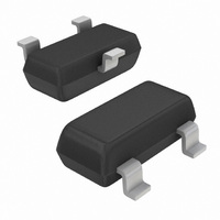
MAX809SN232T1G ON Semiconductor, MAX809SN232T1G Datasheet - Page 3

MAX809SN232T1G
Manufacturer Part Number
MAX809SN232T1G
Description
IC MPU SUPERVISORY 2.32V SOT23
Manufacturer
ON Semiconductor
Type
Simple Reset/Power-On Resetr
Datasheet
1.MAX810MTRG.pdf
(13 pages)
Specifications of MAX809SN232T1G
Number Of Voltages Monitored
1
Output
Push-Pull, Totem Pole
Reset
Active Low
Reset Timeout
140 ms Minimum
Voltage - Threshold
2.32V
Operating Temperature
-40°C ~ 105°C
Mounting Type
Surface Mount
Package / Case
SOT-23-3, TO-236-3, Micro3™, SSD3, SST3
Monitored Voltage
1.2 V to 4.9 V
Undervoltage Threshold
2.32 V
Output Type
Push-Pull
Manual Reset
Not Resettable
Watchdog
No Watchdog
Battery Backup Switching
No Backup
Supply Voltage (max)
5.5 V
Supply Voltage (min)
1 V
Supply Current (typ)
0.8 uA
Maximum Operating Temperature
+ 105 C
Mounting Style
SMD/SMT
Minimum Operating Temperature
- 40 C
Power Fail Detection
No
Number Of Elements
1
Monitored Voltage 1 (typ)
1.2 to 4.9V
Threshold Voltage 1 (max)
2.35V
Watchdog Timer
No
Chip Enable Signals
No
Reset Active Time
460ms
Package Type
SOT-23
Operating Supply Voltage (min)
1.2V
Operating Supply Voltage (max)
5.5V
Reset Threshold Voltage (max)
2.35V
Reset Threshold Voltage (min)
2.28V
Family Name
MAX809
Operating Temp Range
-40C to 105C
Operating Temperature Classification
Industrial
Mounting
Surface Mount
Pin Count
3
Supply Current
0.0025mA
Overvoltage Threshold
2.35 V
Power-up Reset Delay (typ)
460 ms
Lead Free Status / RoHS Status
Lead free / RoHS Compliant
Other names
MAX809SN232T1GOS
Available stocks
Company
Part Number
Manufacturer
Quantity
Price
Company:
Part Number:
MAX809SN232T1G
Manufacturer:
ON
Quantity:
6 000
Part Number:
MAX809SN232T1G
Manufacturer:
ON/安森美
Quantity:
20 000
Stresses exceeding Maximum Ratings may damage the device. Maximum Ratings are stress ratings only. Functional operation above the
Recommended Operating Conditions is not implied. Extended exposure to stresses above the Recommended Operating Conditions may affect
device reliability.
1. This based on a 35x35x1.6mm FR4 PCB with 10mm
2. The maximum package power dissipation limit must not be exceeded.
PIN DESCRIPTION
ABSOLUTE MAXIMUM RATINGS
Power Supply Voltage (V
RESET Output Voltage (CMOS)
Input Current, V
Output Current, RESET
dV/dt (V
Thermal Resistance, Junction−to−Air (Note 1)
Operating Junction Temperature Range
Storage Temperature Range
Lead Temperature (Soldering, 10 Seconds)
ESD Protection
Latchup Current Maximum Rating: Following Specification JESD78 Class II
Pin No.
characterization.
1
2
2
3
CC
P D +
)
Human Body Model (HBM): Following Specification JESD22−A114
RESET (MAX809)
RESET (MAX810)
T J(max) * T A
CC
Machine Model (MM): Following Specification JESD22−A115
Symbol
R qJA
GND
V
CC
CC
to GND)
with T
Rating
Ground
RESET output remains low while V
period after V
RESET output remains high while V
period after V
Supply Voltage (Typ)
J(max)
= 150°C
CC
CC
rises above reset threshold
rises above reset threshold
2
of 1 oz copper traces under natural convention conditions and a single component
http://onsemi.com
3
Negative
SOT−23
Positive
CC
SC−70
CC
is below the reset voltage threshold, and for a reset timeout
is below the reset voltage threshold, and for a reset timeout
Description
Symbol
I
Latchup
R
V
T
T
T
qJA
stg
sol
CC
J
−0.3 to (V
−40 to +105
−65 to +150
−0.3 to 6.0
Value
+260
2000
100
301
314
200
200
200
20
20
CC
+ 0.3)
V/msec
°C/W
Unit
mA
mA
mA
°C
°C
°C
V
V
V


