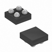
MAX6408BS34+T Maxim Integrated Products, MAX6408BS34+T Datasheet - Page 2

MAX6408BS34+T
Manufacturer Part Number
MAX6408BS34+T
Description
IC DETECTOR VOLT 4-UCSP
Manufacturer
Maxim Integrated Products
Type
Simple Reset/Power-On Resetr
Datasheet
1.MAX6411BS46T.pdf
(8 pages)
Specifications of MAX6408BS34+T
Number Of Voltages Monitored
1
Output
Open Drain or Open Collector
Reset
Active Low
Reset Timeout
20 µs Typical Propagation Delay
Voltage - Threshold
3.4V
Operating Temperature
-40°C ~ 85°C
Mounting Type
Surface Mount
Package / Case
4-UCSP®
Lead Free Status / RoHS Status
Lead free / RoHS Compliant
ABSOLUTE MAXIMUM RATINGS
All voltages measured to GND unless otherwise noted.
VCC ..........................................................................-0.3V to +6V
OUT/OUT ...................................................-0.3V to (V
OUT (open-drain) .....................................................-0.3V to +6V
MR ..............................................................-0.3V to (V
Input/Output Current into Any Pin .......................................20mA
Voltage Detectors in 4-Bump (2
Chip-Scale Package
ELECTRICAL CHARACTERISTICS
(V
Stresses beyond those listed under “Absolute Maximum Ratings” may cause permanent damage to the device. These are stress ratings only, and functional
operation of the device at these or any other conditions beyond those indicated in the operational sections of the specifications is not implied. Exposure to
absolute maximum rating conditions for extended periods may affect device reliability.
2
Supply Voltage Range
Startup Time
Supply Current
Detector Threshold
Voltage Threshold Hysteresis
Detector Threshold Tempco
MR Input
MR Minimum Input Pulse Width
MR Glitch Rejection
MR to OUT/OUT Delay
MR Pullup Resistance
Propagation Delay
OUT Output Voltage Low
(MAX6406/MAX6408/MAX6409/
MAX6411)
OUT Output Voltage High
(MAX6406/MAX6409)
CC
_______________________________________________________________________________________
= 1.0V to 5.5V, T
PARAMETER
A
= -40°C to +85°C, unless otherwise noted. Typical values are at V
SYMBOL
∆V
V
V
V
V
t
I
V
V
V
V
TH
MD
CC
CC
OH
TH
OL
IH
IH
IL
IL
/°C
T
T
MAX6406/MAX6407/MAX6408
V
V
V
Table 1
MAX6406/MAX6407/MAX6408
MAX6409/MAX6410/MAX6411
V
V
V
V
V
I
I
I
OUT not asserted
I
V
I
V
SINK
SINK
SOURCE
SOURCE
SOURCE
A
A
CC
CC
CC
TH
TH
CC
CC
CC
TH
TH
CC
CC
= 0°C to +70°C
= -40°C to +85°C
> 4.0V
≤ 4.0V
≤ 4.38V, OUT not asserted
≥ 4.5V, OUT not asserted
= 3.0V for V
= 3.2V for V
= 5.5V, no load
= (V
= (V
= 0 to V
= 1.6mA, V
= 100µA, V
+ 0.3V)
+ 0.3V)
= 500µA, V
= 800µA, V
= 800µA, V
TH
TH
+ 100mV) to (V
- 100mV) to (V
TH
CONDITIONS
(min)
TH
TH
CC
CC
≤ 2.93V,
> 2.93V, no load
Continuous Power Dissipation (T
Operating Temperature Range ..........................-40°C to +85°C
Junction Temperature ......................................................+150°C
Storage Temperature Range ............................-65°C to +160°C
Bump Reflow Temperature .............................................+235°C
CC
CC
CC
≥ 2.1V, OUT asserted
≥ 1.2V, OUT asserted
4-Pin/Bump UCSP (derate 3.8mW/°C above +70°C)....303mW
T
T
= 3.2V, MAX6406,
= 4.5V,
= V
A
A
= -40°C to +85°C
= +25°C
TH
TH
TH
+ 100mV)
(max),
- 100mV)
X
CC
= 3V and T
2)
V
V
TH
TH
0.7 x V
0.8 x V
0.8 x V
0.8 x V
MIN
1.0
1.2
2.0
25
1
- 1.5% V
- 2.5% V
A
= +70°C)
CC
CC
CC
CC
A
= +25°C.) (Note1)
TYP
100
200
0.5
1.0
6.3
9.5
40
50
20
42
88
TH
TH
V
V
0.2 x V
TH
TH
+ 1.5%
+ 2.5%
MAX
1.75
5.5
5.5
1.0
0.8
0.3
0.4
75
CC
UNITS
ppm/°C
mV
µA
kΩ
µs
ns
ns
µs
µs
V
V
V
V
V


