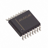
MAX696CWE+ Maxim Integrated Products, MAX696CWE+ Datasheet - Page 12

MAX696CWE+
Manufacturer Part Number
MAX696CWE+
Description
IC SUPERVISOR MPU 16-SOIC
Manufacturer
Maxim Integrated Products
Type
Battery Backup Circuitr
Datasheet
1.MAX696EWE.pdf
(15 pages)
Specifications of MAX696CWE+
Number Of Voltages Monitored
2
Output
Push-Pull, Push-Pull
Reset
Active High/Active Low
Reset Timeout
35 ms Minimum
Voltage - Threshold
Adjustable/Selectable
Operating Temperature
0°C ~ 70°C
Mounting Type
Surface Mount
Package / Case
16-SOIC (0.300", 7.5mm Width)
Monitored Voltage
3 V to 5.5 V
Undervoltage Threshold
Adj V
Overvoltage Threshold
Adj V
Manual Reset
No
Watchdog
Yes
Battery Backup Switching
Yes
Power-up Reset Delay (typ)
70 ms
Supply Voltage (max)
5.5 V
Supply Voltage (min)
3 V
Supply Current (typ)
300 uA
Maximum Power Dissipation
600 mW
Mounting Style
SMD/SMT
Maximum Operating Temperature
+ 70 C
Chip Enable Signals
No
Minimum Operating Temperature
0 C
Output Type
Active High or Active Low or Push-Pull
Power Fail Detection
Yes
Lead Free Status / RoHS Status
Lead free / RoHS Compliant
Microprocessor Supervisory Circuits
Since the power-fail comparator circuit is noninverting,
hysteresis can be added by connecting a resistor
between the PFO output and the PFI input as shown in
Figure 7. When PFO is low, resistor R3 sinks current
from the summing junction at the PFI pin. When PFO is
high, the series combination of R3 and R4 source cur-
rent into the PFI summing junction.
The watchdog feature can be enabled and disabled
under program control by driving WDI with a three-state
Figure 9. Selecting Internal or External Watchdog Timeout
12
Figure 7. Adding Hysteresis to the Power-Fail Voltage
Comparator
Alternate Watchdog Input Drive Circuits
______________________________________________________________________________________
V
V
HYSTERESIS = 1.23V
H
L
= 7.9V
= 9.125V
7V - 15V
Adding Hysteresis to the Power-Fail
R1
75kΩ
R2
13kΩ
Applications Information
7805
R3
300kΩ
+5V
V = 1.3V
V = 1.3V
HYSTERESIS ≈ 5V x R1
ASSUMING R4 << R3
H
L
R4
10kΩ
LOW = INTERNAL
HI = EXTERNAL
WHEN INTERNAL
100ms TIMEOUT
CONNECT FOR
{
{
TIMEOUT
WATCHDOG
TIMEOUT IS
SELECTED
1 +
1 +
WATCHDOG TIMEOUT
V
PFO
PFI
CC
R1
R2
R1
R2
R3
+
+
1.3V (R3 + R4)
(5V - 1.3V) R1
Comparator
MAX696
MAX697
R1
R3
}
TO µP
GND
}
buffer (Figure 8). The drawback to this circuit is that a
software fault may erroneously three-state the buffer,
thereby preventing the MAX696/MAX697 from detect-
ing that the microprocessor is no longer working. In
most cases, a better method is to extend the watchdog
period rather than disabling the watchdog. See Figure
9. When the control input is high, the OSC SEL pin is
low and the watchdog timeout is set by the external
capacitor. A 0.01µF capacitor sets a watchdog timeout
delay of 100s. When the control input is low, the OSC
SEL pin is driven high, selecting the internal oscillator.
The 100ms or the 1.6s period is chosen, depending on
which diode in Figure 9 is used.
Figure 8. Disabling the Watchdog Under Program Control
CONNECT FOR
1.6s INTERNAL
TIMEOUT
WATCHDOG
WATCHDOG
STROBE
DISABLE
OSC SEL
OSC IN
MAX696
MAX697
+5V
V
GND
CC
EN
WDI
MAX696
MAX697
+5V
V
GND
CC


