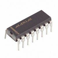
DS1236A-10+ Maxim Integrated Products, DS1236A-10+ Datasheet

DS1236A-10+
Specifications of DS1236A-10+
Related parts for DS1236A-10+
DS1236A-10+ Summary of contents
Page 1
... When an out-of-tolerance condition occurs, the microprocessor reset and power-fail outputs are forced active, and static RAM control unconditionally write protects external memory. The DS1236A also provides early warning detection of a user-defined threshold by driving a non-maskable interrupt. External reset control is provided by a pushbutton reset ...
Page 2
... Reset control and wake-up/sleep control inputs also provide the necessary signals for orderly shutdown and start-up in battery backup and battery operated applications. A block diagram of the DS1236A is shown in NO TAG. PIN DESCRIPTION ...
Page 3
... Independent of the state of the RC pin, the watchdog is also disabled as soon falls CCTP PUSHBUTTON RESET An input pin is provided on the DS1236A for direct connection to a pushbutton. The pushbutton reset input requires an active low signal. Internally, this input is pulled high by a 10k resistor whenever V greater than V . The PBRST BAT driven to the active state for 25 ms minimum ...
Page 4
... RST or . RST When the supply being monitored decays to the voltage sense point, the DS1236A pulses the to the active state for a minimum of 200 μs. The domain hysteresis. That is, the monitored supply is sampled periodically at a rate determined by an internal ring oscillator running at approximately 30 kHz (33 μs/cycle). Three consecutive samplings of out-of-tolerance supply (below V must be below the voltage sense point for approximately 100 μ ...
Page 5
... DS1236A FUNCTIONAL BLOCK DIAGRAM Figure DS1236A ...
Page 6
... POWER SWITCHING When larger operating currents are required in a battery backed system, the 5-volt supply and battery supply switches internal to the DS1236A may not be large enough to support the required load through V with a reasonable voltage drop. For these applications, the PF and CCO external power switching devices ...
Page 7
... ST/INPUT TIMING Figure 2 NMI/FROM ST/INPUT Figure DS1236A ...
Page 8
... POWER MONITOR, WATCHDOG Figure 4 PUSHBUTTON RESET TIMING Figure DS1236A ...
Page 9
... NON-MASKABLE INTERRUPT Figure 6 EXAMPLE 1: 5-VOLT SUPPLY 10k OHM, V ∴ 4.80 = EXAMPLE 2: 12-VOLT SUPPLY 10k OHM, V ∴ 9.00 = NONVOLATILE SRAM Figure 10k X 2.54 10k R1 + 10k X 2.54 10k 9. 5.00 = 17.7 VOLTS MAX 2. DS1236A = 4.80 VOLTS SENSE R1 = 8.9k OHM = 9.00 VOLTS SENSE R1 = 25.4k OHM ...
Page 10
... When the RC pin is tied to ground, the DS1236A is designed to interface with NMOS processors which do not have the microamp currents required during a battery backed mode. Grounding the RC pin does, however, continue to support nonvolatile backup of system SRAM memory. Nonvolatile systems incorporating NMOS processors generally require that only the SRAM memory and/or timekeeping functions be battery backed ...
Page 11
... PBRST then be restarted as the watchdog times out and drives RST and started up by forcing the WC/ SC sleep mode by the processor and system power is lost, the DS1236A will wake up the next time V above V . These possibilities are illustrated in Figure 14. BAT When the sleep mode is invoked during normal power-valid conditions, all operation on the DS1236A is ...
Page 12
... RC pin is tied high (CMOS mode). Subsequent power-up of the V TP with the RC pin tied high will activate the RST and high-to-low transition on the WC/ invoke a Sleep mode for the DS1236A. POWER SWITCHING Figure 8 outputs as the main supply rises above V RST pin must follow a high-to-low transition on the ST pin by t ...
Page 13
... CMOS MODE POWER-DOWN ( Figure 9 CCO DS1236A ...
Page 14
... NMOS MODE POWER-DOWN (RC = GND) Figure DS1236A ...
Page 15
... NMOS MODE POWER-UP (RC = GND) Figure DS1236A ...
Page 16
... CMOS MODE POWER-UP ( Figure 12 CCO DS1236A ...
Page 17
... WAKE/SLEEP CONTROL Figure 13 OPTIONS FOR INVOKING WAKEUP Figure DS1236A ...
Page 18
... MIN TYP BAT I CC01 I CC02 V V -0.3 CCO -0.7 CCO BAT -0.5V V -0. -0.7 OHL BAT R 10k PBRST DS1236A + 0.5V CC (0°C to 70°C) MAX UNITS NOTES 4.5V to 5.5V) CC MAX UNITS NOTES μA 20 μA 0.1 2 100 ...
Page 19
... FB1 t 100 FB2 t .1 REC 100 400 PPF t STN t NRT t ARST t 30 100 BRST SYMBOL MIN TYP OUT DS1236A MAX UNITS NOTES 4. 4. μA +1.0 2 4.5V to 5.5V) CC MAX UNITS NOTES μs 175 μs 175 150 ms μs 500 μ μ 100 ...
Page 20
... CCO 25° the maximum average load which the DS1236A can supply at V CCO1 during normal 5-volt operation the maximum average load which the DS1236A can supply through the V CCO2 retention battery supply operation, with a maximum drop of 0.8 volts μs. 5. With approximately V ...


