MCP1824T-2502E/DC Microchip Technology, MCP1824T-2502E/DC Datasheet - Page 7
MCP1824T-2502E/DC
Manufacturer Part Number
MCP1824T-2502E/DC
Description
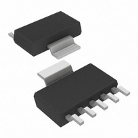
IC LDO REG 300MA 2.5V SOT223-5
Manufacturer
Microchip Technology
Datasheet
1.MCP1824T-1802EOT.pdf
(34 pages)
Specifications of MCP1824T-2502E/DC
Regulator Topology
Positive Fixed
Voltage - Output
2.5V
Voltage - Input
Up to 6V
Voltage - Dropout (typical)
0.2V @ 300mA
Number Of Regulators
1
Current - Output
300mA (Min)
Operating Temperature
-40°C ~ 125°C
Mounting Type
Surface Mount
Package / Case
SOT-223 (5 leads + Tab)
Primary Input Voltage
2.82V
Output Voltage
2.5V
Dropout Voltage Vdo
200mV
No. Of Pins
5
Output Current
300mA
Voltage Regulator Case Style
SOT-223
Operating Temperature Range
-40°C To
Number Of Outputs
1
Polarity
Positive
Input Voltage Max
6 V
Output Type
Fixed
Dropout Voltage (max)
0.32 V at 300 mA
Line Regulation
0.05 % / V
Load Regulation
0.5 %
Voltage Regulation Accuracy
2.5 %
Maximum Operating Temperature
+ 125 C
Mounting Style
SMD/SMT
Minimum Operating Temperature
- 40 C
Output Voltage Fixed
2.5V
Rohs Compliant
Yes
Lead Free Status / RoHS Status
Lead free / RoHS Compliant
Current - Limit (min)
-
Lead Free Status / Rohs Status
Lead free / RoHS Compliant
Other names
MCP1824T-2502E/DCTR
Available stocks
Company
Part Number
Manufacturer
Quantity
Price

Part Number:
MCP1824T-2502E/DC
Manufacturer:
SOT-223
Quantity:
20 000


1.0
Absolute Maximum Ratings †
Input Voltage, V
Maximum Voltage on Any Pin ... (GND – 0.3V) to (V
Maximum Power Dissipation......... Internally-Limited (Note 6)
Output Short Circuit Duration ................................ Continuous
Storage temperature .....................................-65°C to +150°C
Maximum Junction Temperature, T
Operating Junction Temperature, T
EESD protection on all pins
AC/DC CHARACTERISTICS
Electrical Specifications: Unless otherwise noted, V
I
Boldface type applies for junction temperatures, T
Input Operating Voltage
Output Voltage Range
Input Quiescent Current
Input Quiescent Current for
SHDN Mode
Maximum Continuous Output
Current
Line Regulation
Load Regulation
Output Short Circuit Current
Dropout Voltage
Pulsed Applications
Maximum Pulsed Output
Current
Note 1:
OUT
2007 Microchip Technology Inc.
= 1 mA, C
2:
3:
4:
5:
6:
7:
ELECTRICAL
CHARACTERISTICS
Parameters
The minimum V
V
voltage for the adjustable cases. V
TCV
temperature range. V
Load regulation is measured at a constant junction temperature using low duty-cycle pulse testing. Load regulation is
tested over a load range from 1 mA to the maximum specified output current.
Dropout voltage is defined as the input-to-output voltage differential at which the output voltage drops 2% below its
nominal value that was measured with an input voltage of V
The maximum allowable power dissipation is a function of ambient temperature, the maximum allowable junction
temperature and the thermal resistance from junction to air. (i.e., T
dissipation will cause the device operating junction temperature to exceed the maximum +150°C rating. Sustained
junction temperatures above 150°C can impact device reliability.
The junction temperature is approximated by soaking the device under test at an ambient temperature equal to the
desired junction temperature. The test time is small enough such that the rise in the junction temperature over the
ambient temperature is not significant.
R
IN
IN
is the nominal regulator output voltage for the fixed cases. V
OUT
.............................................................6.5V
= C
OUT
= (V
OUT-HIGH
= 4.7 µF (X7R Ceramic), T
........... ≥
IN
must meet two conditions: V
OUT-LOW
J
J
– V
........................... +150°C
.............-40°C to +125°C
(V
ΔV
4 kV HBM;
V
OUT
OUT-LOW
I
ΔV
DROPOUT
OUT
OUT_SC
I
I
V
PULSE
Sym
SHDN
I
V
OUT
OUT
I
OUT
x ΔV
is the lowest voltage measured over the temperature range.
IN
q
/V
OUT
/
R
) *10
IN
≥
= V
)
J
IN
300V MM
6
(Note 7) of -40°C to +125°C
ADJ *
A
+ 0.3)V
/ (V
IN
= +25°C.
= V
Min
-1.0
300
R
2.1
0.8
((R
—
—
—
—
—
—
* ΔTemperature). V
IN
OUT(MAX)
1
≥ 2.1V and V
/R
2
)+1).
±0.05
±0.5
Typ
120
720
200
500
+ V
0.1
—
—
—
Figure
MCP1824/MCP1824S
ings” may cause permanent damage to the device. This is a
stress rating only and functional operation of the device at
those or any other conditions above those indicated in the
operational listings of this specification is not implied. Expo-
sure to maximum rating conditions for extended periods may
affect device reliability.
† Notice: Stresses above those listed under “Maximum Rat-
IN
DROPOUT(MAX)
IN
= V
R
4-1.
≥ V
= 1.2V, 1.8V, etc. V
OUT-HIGH
OUT(MAX)
A
, T
±0.17
Max
220
320
OUT(MAX)
6.0
5.0
1.0
J
—
—
—
3
, θ
JA
, Note 1, V
). Exceeding the maximum allowable power
is the highest voltage measured over the
+ V
+ V
DROPOUT(MAX)
Units
%/V
mA
mA
mV
mA
µA
µA
%
V
V
DROPOUT(MAX).
R
R
is the desired set point output
= 1.8V for Adjustable Output,
I
5.0V
SHDN = GND
V
V
(Note 1) ≤ V
I
R
Note 5, I
V
V
V
Duty Cycle ≤ 60%,
Period < 10 ms
L
OUT
(Note 4)
IN
R
IN(MIN)
IN
R
LOAD
= 0 mA, V
= 0.8V to 5.0V
= 0.8V to 5.0V,
= 2.1V to 6.0V
= 2.1V to 6.0V
.
= 1 mA to 300 mA,
< 0.1Ω, Peak Current
= 2.1V
OUT
Conditions
OUT
DS22070A-page 7
IN
= 300 mA,
≤ 6V
= 0.8V to
Related parts for MCP1824T-2502E/DC
Image
Part Number
Description
Manufacturer
Datasheet
Request
R

Part Number:
Description:
IC LDO REG 300MA 3.3V SOT23-5
Manufacturer:
Microchip Technology
Datasheet:
Part Number:
Description:
IC LDO REG 300MA 1.8V SOT23-5
Manufacturer:
Microchip Technology
Datasheet:
Part Number:
Description:
IC LDO REG 300MA 5.0V SOT23-5
Manufacturer:
Microchip Technology
Datasheet:
Part Number:
Description:
IC LDO REG 300MA 2.5V SOT23-5
Manufacturer:
Microchip Technology
Datasheet:
Part Number:
Description:
IC LDO REG 300MA 3.0V SOT23-5
Manufacturer:
Microchip Technology
Datasheet:

Part Number:
Description:
IC LDO REG 300MA 3.3V SOT223-5
Manufacturer:
Microchip Technology
Datasheet:
Part Number:
Description:
IC LDO REG 300MA 5.0V SOT223-5
Manufacturer:
Microchip Technology
Datasheet:
Part Number:
Description:
IC LDO REG 300MA 3.0V SOT223-5
Manufacturer:
Microchip Technology
Datasheet:
Part Number:
Description:
IC LDO REG 300MA ADJ-V SOT223-5
Manufacturer:
Microchip Technology
Datasheet:
Part Number:
Description:
IC REG LDO 300MA 1.8V SOT223-5
Manufacturer:
Microchip Technology
Datasheet:
Part Number:
Description:
IC REG LDO 300MA 1.2V SOT223-5
Manufacturer:
Microchip Technology
Datasheet:
Part Number:
Description:
IC LDO REG 300MA ADJ-V SOT23-5
Manufacturer:
Microchip Technology
Datasheet:
Part Number:
Description:
IC REG LDO 300MA 1.2V SOT23-5
Manufacturer:
Microchip Technology
Datasheet:
Part Number:
Description:
IC REG LDO 300MA 0.8V SOT23-5
Manufacturer:
Microchip Technology
Datasheet:
Part Number:
Description:
300 MA CMOS LDO, Vout=0.8V, Extended Temp Range 5 SOT-223 T/R
Manufacturer:
Microchip Technology
Datasheet: