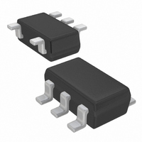
XC6210B332MR Torex Semiconductor Ltd, XC6210B332MR Datasheet

XC6210B332MR
Specifications of XC6210B332MR
Available stocks
Related parts for XC6210B332MR
XC6210B332MR Summary of contents
Page 1
Power Consumption ◆Maximum Output Current :More than 700mA ◆Dropout Voltage ◆Operating Voltage Range ◆Output Voltage Range ◆Low ESR Capacitor Compatible ■GENERAL DESCRIPTION The XC6210 series are precise, low noise, high current, positive voltage low dropout regulators. They are ...
Page 2
XC6210 Series ■PIN CONFIGURATION VOUT VIN VSS CE SOT-25 (TOP VIEW) ■PIN ASSIGNMENT PIN NUMBER SOT-25 SOT-89 ■PRODUCT CLASSIFICATION ●Selection Guide CE Input Logic, ...
Page 3
INFORMATION ●SOT-25 (SOT-23-5) 2.9+0.2 5-0.4 +0.1 -0.05 0.95 0.95 1.9+0.2 ●USP-6B Data Sheet un200533 ●SOT-89-5 4.5+0.1 0.42+0.06 0.42+0.06 0~0.1 0.15 +0.1 0.42+0.06 0.47+0.06 -0. 1.5+0.1 * Pin no thicker than other pins. XC6210 +0.03 0.4 ...
Page 4
XC6210 Series ■MARKING RULE ●SOT-25 1Represents product series 5 4 ① ② ③ ④ 2Represents CE function VOLTAGE=0.1~3.0V ●SOT-89 3Represents output voltage MARK SOT-89-5 4 (TOP VIEW) ...
Page 5
DIAGRAM ON/OFF CE Control - Error Amp + ■ABSOLUTE MAXIMUM RATINGS PARAMETER Input Voltage Output Current * Output Voltage CE Pin Voltage SOT-25 Power Dissipation SOT-89-5 USP-6B Operating Temperature Range Storage Temperature Range * I = – ...
Page 6
XC6210 Series ■ELECTRICAL CHARACTERISTICS ●XC6210 series PARAMETER SYMBOL Output Voltage (*2), (*3) V (E) OUT Maximum Output Current I OUTMAX [V (E)>1.6V] OUT Maximum Output Current I OUTMAX [V (E)<1.5V] OUT Load Regulation △V OUT Vdif1 Dropout Voltage (*4) Vdif2 ...
Page 7
CHART ●Dropout Voltage, Supply Current, CE “H / L” Level Current Chart OUTPUT SETTING DROPOUT VOLTAGE OUTPUT VOLTAGE 1 (Accuracy: 2%) VOLTAGE (I OUT (V) (V) V OUT V (T) OUT MIN. MAX. TYP. 0.80 0.770 0.830 100.0 0.90 ...
Page 8
XC6210 Series ■VOLTAGE CHART (Continued) ●Dropout Voltage, Supply Current, CE “H / L” Level Current Chart OUTPUT SETTING DROPOUT VOLTAGE OUTPUT VOLTAGE 1 (Accuracy: 2%) VOLTAGE (I OUT (V) (V) V OUT V OUT(T) MIN. MAX. TYP. 3.00 2.940 3.060 ...
Page 9
CIRCUITS ●Circuit ●Circuit 2 3 ●Circuit VIN={VOUT+1.0V}VDC+0.5Vp-pAC VOUT>4.75V VOUT≧4.75V VIN=5.75VDC+0.5Vp-pAC ●Output Capacitor Corresponding Chart VR OUTPUT VOLTAGE C L Data Sheet un200533 V IN CIN VCE ...
Page 10
XC6210 Series ■OPERATIONAL EXPLANATION <Output Voltage Regulator Control> The voltage, divided by resistors R1 & R2, which are connected to the V reference voltage by the error amplifier. The P-channel MOSFET, which is connected to the V driven by the ...
Page 11
PERFORMANCE CHARACTERISTICS (1) Output Voltage vs. Output Current XC6210 (VOUT:0.8V) CIN=1.0uF(ceramic),CL=6.8uF(ceramic) 0.9 0.8 0.7 0.6 Ta=-40 ℃ Ta=25 ℃ 0.5 Ta=85 ℃ 0.4 0.3 0.2 0 100 200 300 400 500 Output Current:IOUT(mA) XC6210 (VOUT:3.0V) CIN=1.0uF(ceramic),CL=1.0uF(ceramic) 4.0 ...
Page 12
XC6210 Series ■TYPICAL PERFORMANCE CHARACTERISTICS (Continued) (2) Output Voltage vs. Input Voltage XC6210 (VOUT:0.8V) CIN=1.0uF(ceramic),CL=6.8uF(ceramic) 1.1 1.0 0.9 0.8 0.7 0.6 0.5 0.5 1.0 Input Voltage:VIN(V) XC6210 (VOUT:3.0V) CIN=1.0uF(ceramic),CL=1.0uF(ceramic) 3.2 3.0 2.8 2.6 2.4 2.2 2.5 3.0 Input Voltage:VIN(V) XC6210 ...
Page 13
PERFORMANCE CHARACTERISTICS (Continued) (3) Dropout Voltage vs. Output Current XC6210 (VOUT:0.8V) CIN=1.0uF(ceramic),CL=6.8uF(ceramic) 1.0 0.8 Below the minimum operating voltage 0.6 0.4 0.2 0.0 0 100 200 300 Output Current:IOUT(mA) XC6210 (VOUT:1.5V) CIN=1.0uF(ceramic),CL=6.8uF(ceramic) 0.6 0.5 Ta=85 ℃ Ta=25 ℃ 0.4 ...
Page 14
XC6210 Series ■TYPICAL PERFORMANCE CHARACTERISTICS (Continued) (4) Supply Current vs. Input Voltage XC6210 (VOUT:0.8V) CIN=1.0uF(ceramic),CL=6.8uF(ceramic) 100 80 Ta=85 ℃ Ta=25 ℃ 60 Ta=-40 ℃ 0.0 1.0 2.0 3.0 Input Voltage:VIN(V) XC6210 (VOUT:5.0V) CIN=1.0uF(ceramic),CL=1.0uF(ceramic) 120 100 80 60 ...
Page 15
PERFORMANCE CHARACTERISTICS (Continued) (6) Supply Current vs. Ambient Temperature XC6210 (VOUT:0.8V) CIN=1.0uF(ceramic),CL=6.8uF(ceramic -50 - Ambient Temperature:Ta( ℃ ) XC6210 (VOUT:5.0V) CIN=1.0uF(ceramic),CL=1.0uF(ceramic -50 -25 0 ...
Page 16
XC6210 Series ■TYPICAL PERFORMANCE CHARACTERISTICS (Continued) (8) Input Transient Response 1 XC6210 (VOUT:0.8V) CL=6.8uF(ceramic),Ta=25 ℃ 1.2 Input Voltage 1.1 1.0 0.9 0.8 Output Voltage 0.7 0.6 Time (20usec/div) XC6210 (VOUT:3.0V) IOUT=30mA,tr=tf=5.0usec CL=1.0uF(ceramic),Ta=25 ℃ 3.4 Input Voltage 3.3 3.2 3.1 3.0 ...
Page 17
PERFORMANCE CHARACTERISTICS (Continued) (9) Load Transient Response XC6210 (VOUT:0.8V) VIN=1.8V,tr=tf=5.0usec,Ta=25 ℃ CIN=1.0uF(ceramic),CL=6.8uF(ceramic) 1.0 Output Voltage 0.8 0.6 0.4 Output Current 100mA 0.2 10mA 0.0 Time (25usec/div) XC6210 (VOUT:3.0V) VIN=4.0V,tr=tf=5.0usec,Ta=25 ℃ CIN=1.0uF(ceramic),CL=1.0uF(ceramic) 3.4 Output Voltage 3.0 2.6 2.2 Output Current ...
Page 18
XC6210 Series ■TYPICAL PERFORMANCE CHARACTERISTICS (Continued) (10) Ripple Rejection Rate XC6210 (VOUT:0.8V) VIN=1.8VDC+0.5Vp-pAC,IOUT=30mA,Ta=25 ℃ CIN=1.0uF(ceramic),CL=6.8uF(ceramic 0.01 0.1 1 Ripple Frequency:f (kHz) XC6210 (VOUT:5.0V) VIN=5.75VDC+0.5Vp-pAC,IOUT=30mA,Ta=25 ℃ CIN=1.0uF(ceramic),CL=1.0uF(ceramic ...
Page 19
PERFORMANCE CHARACTERISTICS (Continued) (11) Input Transient Response 2 XC6210 (VOUT:0.8V) VIN=1.8V,IOUT=30mA,tr=5.0usec CIN=1.0uF(ceramic),CL=6.8uF(ceramic),Ta=25 ℃ Input Voltage Output Voltage 1 0 Time (25usec/div) XC6210 (VOUT:3.0V) VIN=4.0V,IOUT=30mA,tr=5.0usec CIN=1.0uF(ceramic),CL=1.0uF(ceramic),Ta=25 ℃ Input Voltage 4 3 Output Voltage ...


